


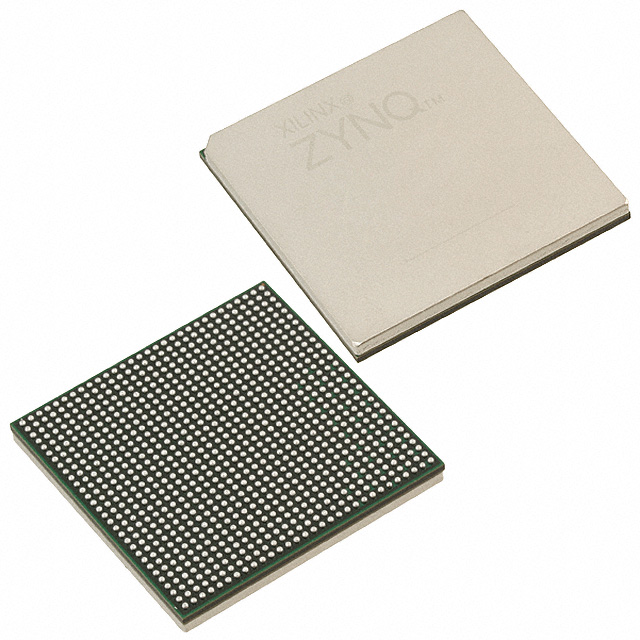

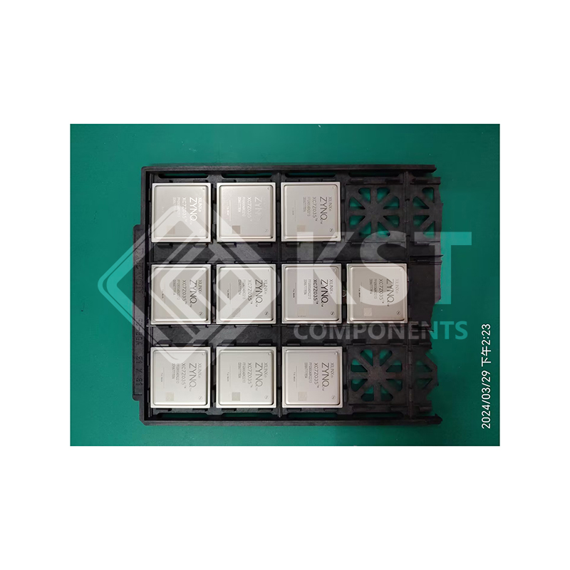

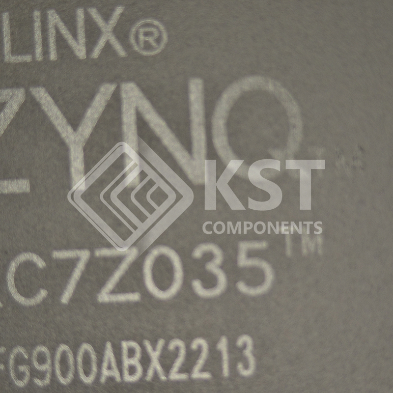
XC7Z035-2FFG900I
INQUIRY ONLINE
ARM Cortex-A9 Based
Application Processor Unit (APU)
• 2.5 DMIPS/MHz per CPU
• CPU frequency: Up to 1 GHz
• Coherent multiprocessor support
• ARMv7-A architecture
• TrustZone® security
• Thumb®-2 instruction set
• Jazelle® RCT execution Environment Architecture
• NEON™ media-processing engine
• Single and double precision Vector Floating Point Unit (VFPU)
• CoreSight™ and Program Trace Macrocell (PTM)
• Timer and Interrupts
• Three watchdog timers
• One global timer
• Two triple-timer counters
Caches
• 32 KB Level 1 4-way set-associative instruction and data caches
(independent for each CPU)
• 512 KB 8-way set-associative Level 2 cache
(shared between the CPUs)
• Byte-parity support
On-Chip Memory
• On-chip boot ROM
• 256 KB on-chip RAM (OCM)
• Byte-parity support
External Memory Interfaces
• Multiprotocol dynamic memory controller
• 16-bit or 32-bit interfaces to DDR3, DDR3L, DDR2, or LPDDR2
memories
• ECC support in 16-bit mode
• 1GB of address space using single rank of 8-, 16-, or 32-bit-wide
memories
• Static memory interfaces
• 8-bit SRAM data bus with up to 64 MB support
• Parallel NOR flash support
• ONFI1.0 NAND flash support (1-bit ECC)
• 1-bit SPI, 2-bit SPI, 4-bit SPI (quad-SPI), or two quad-SPI (8-bit)
serial NOR flash
8-Channel DMA Controller
• Memory-to-memory, memory-to-peripheral, peripheral-to-memory,
and scatter-gather transaction support
I/O Peripherals and Interfaces
• Two 10/100/1000 tri-speed Ethernet MAC peripherals with
IEEE Std 802.3 and IEEE Std 1588 revision 2.0 support
• Scatter-gather DMA capability
• Recognition of 1588 rev. 2 PTP frames
• GMII, RGMII, and SGMII interfaces
• Two USB 2.0 OTG peripherals, each supporting up to 12 Endpoints
• USB 2.0 compliant device IP core
• Supports on-the-go, high-speed, full-speed, and low-speed
modes
• Intel EHCI compliant USB host
• 8-bit ULPI external PHY interface
• Two full CAN 2.0B compliant CAN bus interfaces
• CAN 2.0-A and CAN 2.0-B and ISO 118981-1 standard
compliant
• External PHY interface
• Two SD/SDIO 2.0/MMC3.31 compliant controllers
• Two full-duplex SPI ports with three peripheral chip selects
• Two high-speed UARTs (up to 1 Mb/s)
• Two master and slave I2C interfaces
• GPIO with four 32-bit banks, of which up to 54 bits can be used with
the PS I/O (one bank of 32b and one bank of 22b) and up to 64 bits
(up to two banks of 32b) connected to the Programmable Logic
• Up to 54 flexible multiplexed I/O (MIO) for peripheral pin assignments
Interconnect
• High-bandwidth connectivity within PS and between PS and PL
• ARM AMBA® AXI based
• QoS support on critical masters for latency and bandwidth control
Programmable Logic (PL)
Configurable Logic Blocks (CLB)
• Look-up tables (LUT)
• Flip-flops
• Cascadeable adders
36 Kb Block RAM
• True Dual-Port
• Up to 72 bits wide
• Configurable as dual 18 Kb block RAM
DSP Blocks
• 18 x 25 signed multiply
• 48-bit adder/accumulator
• 25-bit pre-adder
Programmable I/O Blocks
• Supports LVCMOS, LVDS, and SSTL
• 1.2V to 3.3V I/O
• Programmable I/O delay and SerDes
JTAG Boundary-Scan
• IEEE Std 1149.1 Compatible Test Interface
PCI Express® Block
• Supports Root complex and End Point configurations
• Supports up to Gen2 speeds
• Supports up to 8 lanes
Serial Transceivers
• Up to 16 receivers and transmitters
• Supports up to 12.5 Gb/s data rates
Two 12-Bit Analog-to-Digital Converters
• On-chip voltage and temperature sensing
• Up to 17 external differential input channels
• One million samples per second maximum conversion rate