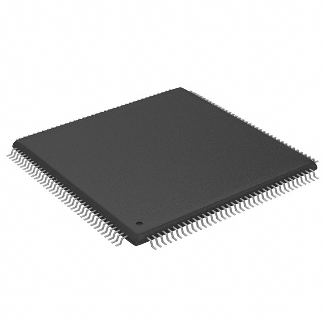
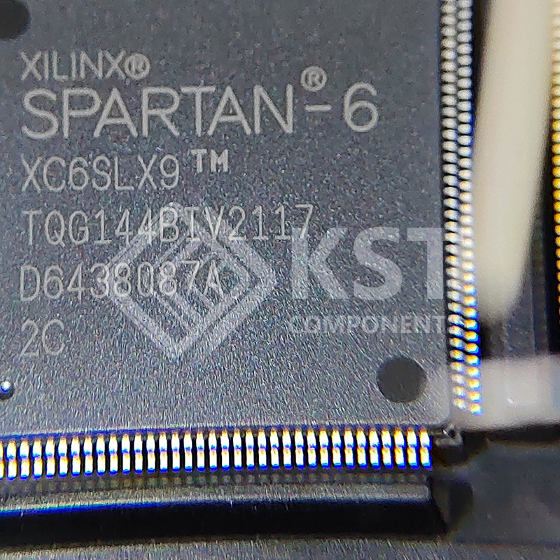
XC6SLX9-2TQG144C

Spartan®-6 LX and LXT FPGAs are available in various speed grades, with -3 having the highest performance. The DC and
AC electrical parameters of the Automotive XA Spartan-6 FPGAs and Defense-grade Spartan-6Q FPGAs devices are
equivalent to the commercial specifications except where noted. The timing characteristics of the commercial (XC) -2 speed
grade industrial device are the same as for a -2 speed grade commercial device. The -2Q and -3Q speed grades are
exclusively for the expanded (Q) temperature range. The timing characteristics are equivalent to those shown for the -2 and
-3 speed grades for the Automotive and Defense-grade devices.
Spartan-6 FPGA DC and AC characteristics are specified for commercial (C), industrial (I), and expanded (Q) temperature
ranges. Only selected speed grades and/or devices might be available in the industrial or expanded temperature ranges for
Automotive and Defense-grade devices. References to device names refer to all available variations of that part number (for
example, LX75 could denote XC6SLX75, XA6SLX75, or XQ6SLX75). The Spartan-6 FPGA -3N speed grade designates
devices that do not support MCB functionality.
All supply voltage and junction temperature specifications are representative of worst-case conditions. The parameters
included are common to popular designs and typical applications.
Available device and package combinations can be found at:
• DS160: Spartan-6 Family Overview
• DS170: Automotive XA Spartan-6 Family Overview
• DS172: Defense-Grade Spartan-6Q Family Overview


Download Details PDF

Notice:

In stock will ship in 2 days. Real-time inventory pls confirm with us.

INQUIRY ONLINE


    SPECIFICATION

    1. All voltages are relative to ground.
    2. See Interface Performances for Memory Interfaces in Table 25. The extended performance range is specified for designs not using the
    standard VCCINT voltage range. The standard VCCINT voltage range is used for:
    • Designs that do not use an MCB
    • LX4 devices
    • Devices in the TQG144 or CPG196 packages
    • Devices with the -3N speed grade
    3. Recommended maximum voltage droop for VCCAUX is 10 mV/ms.
    4. During configuration, if VCCO_2 is 1.8V, then VCCAUX must be 2.5V.
    5. The -1L devices require VCCAUX = 2.5V when using the LVDS_25, LVDS_33, BLVDS_25, LVPECL_25, RSDS_25, RSDS_33, PPDS_25,
    and PPDS_33 I/O standards on inputs. LVPECL_33 is not supported in the -1L devices.
    6. Configuration data is retained even if VCCO drops to 0V.
    7. Includes VCCO of 1.2V, 1.5V, 1.8V, 2.5V, and 3.3V.
    8. For PCI systems, the transmitter and receiver should have common supplies for VCCO.
    9. Devices with a -1L speed grade do not support Xilinx PCI IP.
    10. Do not exceed a total of 100 mA per bank.
    11. VBATT is required to maintain the battery backed RAM (BBR) AES key when VCCAUX is not applied. Once VCCAUX is applied, VBATT can be
    unconnected. When BBR is not used, Xilinx recommends connecting to VCCAUX or GND. However, VBATT can be unconnected