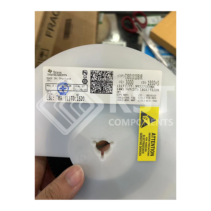
TXB0101DBVR

This 1-bit noninverting translator uses two separate
configurable power-supply rails. The A port is
designed to track VCCA. VCCA accepts any supply
voltage from 1.2 V to 3.6 V. The B port is designed
to track VCCB. VCCB accepts any supply voltage from
1.65 V to 5.5 V. This allows for universal low-voltage
bidirectional translation between any of the 1.2-V, 1.5-
V, 1.8-V, 2.5-V, 3.3-V, and 5-V voltage nodes. VCCA
should not exceed VCCB.
When the output-enable (OE) input is low, all outputs
are placed in the high-impedance state.
This device is fully specified for partial-power-down
applications using Ioff. The Ioff circuitry disables
the outputs, preventing damaging current backflow
through the device when it is powered down.
To ensure the high-impedance state during power up
or power down, OE should be tied to GND through a
pulldown resistor; the minimum value of the resistor
is determined by the current-sourcing capability of the
driver.
NanoFree™ package technology is a major
breakthrough in IC packaging concepts, using the die
as the package.

Category:

Download Details PDF

Notice:

In stock will ship in 2 days. Real-time inventory pls confirm with us.

INQUIRY ONLINE


    SPECIFICATION

    • Available in the Texas Instruments NanoFree™
    package
    • 1.2 V to 3.6 V on A port and
    1.65 V to 5.5 V on B port (VCCA ≤ VCCB)
    • VCC isolation feature – if either VCC input is at
    GND, all outputs are in the high-impedance state
    • OE input circuit referenced to VCCA
    • Low power consumption, 5 μA maximum ICC
    • Ioff supports partial-power-down mode operation
    • Latch-up performance exceeds 100 mA Per JESD
    78, class II
    • ESD protection Exceeds JESD 22
    – A port
    • 2000 V Human body model (A114-B)
    • 250 V Machine model (A115-A)
    • 1500 V Charged-device model (C101)
    – B port
    • 15 kV Human body model (A114-B)
    • 250 V Machine model (A115-A)
    • 1500 V Charged-device model (C101)