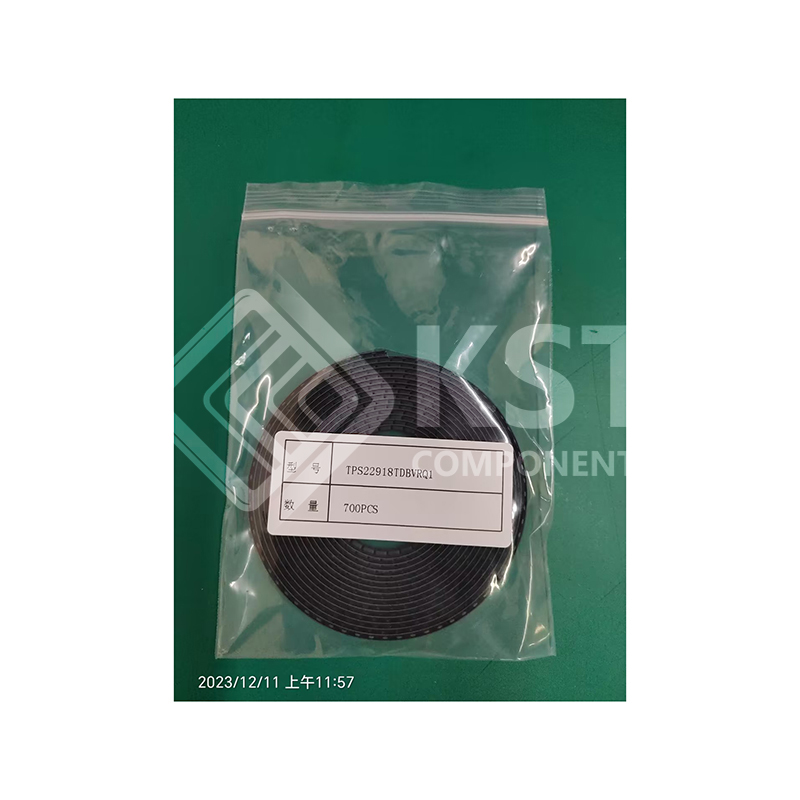
TPS22918TDBVRQ1

The TPS22918-Q1 is a single-channel load switch
with both configurable rise time and configurable
quick-output discharge. The device contains an Nchannel MOSFET that can operate over an input
voltage range of 1 V to 5.5 V and can support a
maximum continuous current of
2 A. The switch is controlled by an on and off input,
which is capable of interfacing directly with lowvoltage control signals.
The configurable rise time of the device reduces
inrush current caused by large bulk load
capacitances, thereby reducing or eliminating power
supply droop. The TPS22918-Q1 features a
configurable quick output discharge (QOD) pin, which
controls the fall time of the device to allow design
flexibility for power down and sequencing.
The TPS22918-Q1 is available in a small, leaded
SOT-23 package (DBV) which allows to visually
inspect solder joints. The device is characterized for
operation over the free-air temperature range of
–40°C to +105°C


Download Details PDF

Notice:

In stock will ship in 2 days. Real-time inventory pls confirm with us.

INQUIRY ONLINE


    SPECIFICATION

    1• AEC-Q100 Qualified
    • Integrated single-channel load switch
    • Qualified for automotive applications:
    – Device Temperature Grade 2: –40°C to
    +105°C ambient operating temperature range
    • Functional safety capable
    – Documentation available to aid functional
    safety system design
    • Input voltage range: 1 V to 5.5 V
    • Low On-Resistance (RON)
    – RON = 52 mΩ (typical) at VIN = 5 V
    – RON = 53 mΩ (typical) at VIN = 3.3 V
    • 2-A Maximum continuous switch current
    • Low quiescent current
    – 8.3 µA (typical) at VIN = 3.3 V
    • Low-control input-threshold enables use of 1 V or
    higher GPIO
    • Configurable Quick-Output Discharge (QOD)
    • Configurable rise time with CT pin
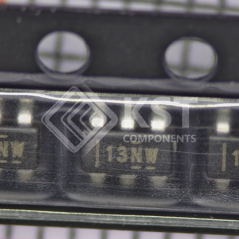
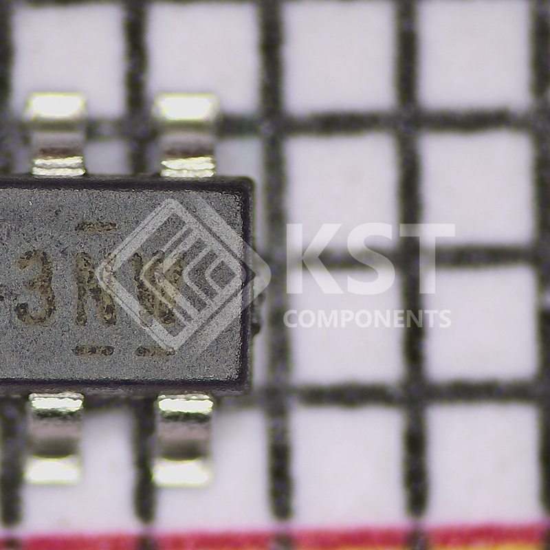
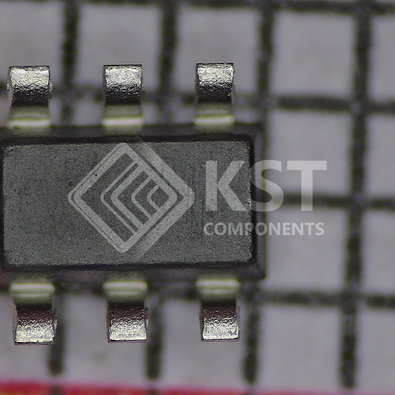
    • Small SOT23-6 package (DBV)
    – 2.9 mm × 2.8 mm, 0.95-mm Pitch,
    1.45-mm height (with leads)
    • ESD Performance tested per AEC Q100
    – ±2-kV HBM and ±750-V CDM