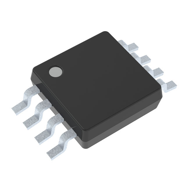
TCA9406DCUR

The TCA9406 is a 2-bit bidirectional I
2C and SMBus
voltage-level translator with an output enable (OE)
input. It is operational from 1.65 V to 3.6 V on the Aside, referenced toVCCA, and from 2.3 V to 5.5 V on
the B-side, referenced to VCCB. This allows the device
to interface between lower and higher logic signal
levels at any of the typical 1.8-V, 2.5-V, 3.3-V, and
5-V supply rails.
The OE input pin is referenced to VCCA, can be tied
directly to VCCA, but it is also 5.5-V tolerant. The OE
pin can also be controlled and set to a logic low to
place all the SCL and SDA pins in a high-impedance
state, which significantly reduces the quiescent
current consumption.
Under normal I
2C and SMBus operation or other
open-drain configurations, the TCA9406 can support
up to 2 Mbps; therefore, it is compatible with standard
I
2C speeds where the frequency of SCL is 100 kHz
(Standard-mode), 400 kHz (Fast-mode), or 1 MHz
(Fast-mode Plus). The device can also be used as a
general purpose level translator, and when the A- and
B-side ports are both driven with push-pull devices
the TCA9406 can support up to 24 Mbps.
The TCA9406 features internal 10-kΩ pullup resistors
on SCL_A, SDA_A, SCL_B, and SDA_B. Additional
external pullup resistors can be added to the bus to
reduce the total pullup resistance and speed up rising
edges.

Category:

Download Details PDF

Notice:

In stock will ship in 2 days. Real-time inventory pls confirm with us.

INQUIRY ONLINE


    SPECIFICATION

    • 2-Bit Bidirectional Translator for SDA and SCL
    Lines in I
    2C Applications
    • Provides Bidirectional Voltage Translation With No
    Direction Pin
    • High-Impedance Output SCL_A, SDA_A, SCL_B,
    SDA_B Pins When OE = Low or VCC = 0 V
    • Internal 10-kΩ Pullup Resistor on All SDA and
    SCL Pins
    • 1.65 V to 3.6 V on A port and 2.3 V to 5.5 V on B
    port (VCCA ≤ VCCB)
    • VCC Isolation Feature: If Either VCC Input Is at
    GND, Both Ports Are in the High-Impedance State
    • No Power-Supply Sequencing Required: Either
    VCCA or VCCB Can Be Ramped First
    • Low Ioff of 2 µA When Either VCCA or VCCB = 0 V
    • OE Input Can Be Tied Directly to VCCA Or
    Controlled By GPIO
    • Latch-Up Performance Exceeds 100 mA Per
    JESD 78, Class II
    • ESD Protection Exceeds JESD 22
    – A Port
    – 2500-V Human-Body Model (A114-B)
    – 250-V Machine Model (A115-A)
    – 1500-V Charged-Device Model (C101)
    – B Port
    – 8-kV Human-Body Model (A114-B)
    – 250-V Machine Model (A115-A)
    – 1500-V Charged-Device Model (C101)