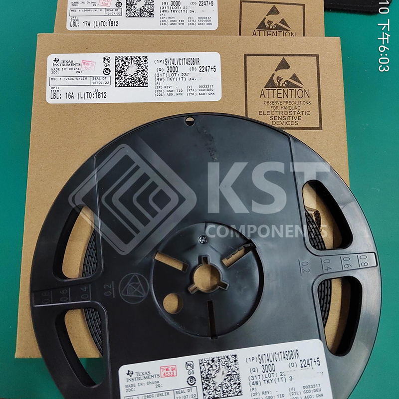
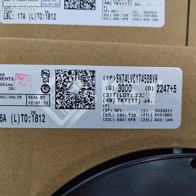
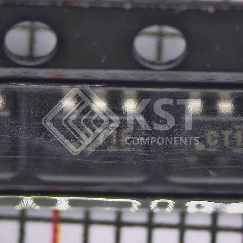
SN74LVC1T45DBVR

This single-bit noninverting bus transceiver uses two
separate configurable power-supply rails. The A port
is designed to track VCCA. VCCA accepts any supply
voltage from 1.65V to 5.5V. The B port is designed
to track VCCB. VCCB accepts any supply voltage from
1.65V to 5.5V. This allows for universal low-voltage
bidirectional translation between any of the 1.8V, 2.5V,
3.3V, and 5V voltage nodes.
The SN74LVC1T45 is designed for asynchronous
communication between two data buses. The logic
levels of the direction-control (DIR) input activate
either the B-port outputs or the A-port outputs. The
device transmits data from the A bus to the B bus
when the B-port outputs are activated and from the
B bus to the A bus when the A-port outputs are
activated. The input circuitry is always active on both
A and B ports and must have a logic HIGH or LOW
level applied to prevent excess ICC and ICCZ.
The SN74LVC1T45 is designed so that the DIR input
is powered by VCCA. This device is fully specified
for partial-power-down applications using Ioff. The Ioff
circuitry disables the outputs, preventing damaging
current backflow through the device when it is
powered down. The VCC isolation feature is designed
so that if either VCC input is at GND, then both ports
are in the high-impedance state.
NanoFree™ package technology is a major
breakthrough in IC packaging concepts, using the die
as the package.

Category:

Download Details PDF

Notice:

In stock will ship in 2 days. Real-time inventory pls confirm with us.

INQUIRY ONLINE


    SPECIFICATION

    • ESD protection exceeds JESD 22:
    – 2000V Human-Body Model (A114-A)
    – 200V Machine Model (A115-A)
    – 1000V Charged-Device Model (C101)
    • Available in the Texas Instruments NanoFree™
    package
    • Fully configurable dual-rail design allows each port
    to operate over the full 1.65V to 5.5V power-supply
    range
    • VCC isolation feature – if either VCC input is at
    GND, both ports are in the high-impedance state
    • DIR input circuit referenced to VCCA
    • Low power consumption, 4µA maximum ICC
    • ±24mA output drive at 3.3V
    • Ioff supports partial-power-down mode operation
    • Maximum data rates
    – 420Mbps (3.3V to 5V translation)
    – 210Mbps (translate to 3.3V)
    – 140Mbps (translate to 2.5V)
    – 75Mbps (translate to 1.8V)
    • Latch-up performance exceeds 100mA per JESD
    78, Class II