SN74LVC1G125DCKR

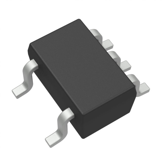
This bus buffer gate is designed for 1.65-V to 5.5-V VCC operation.

The SN74LVC1G125 device is a single line driver with a 3-state output. The output is disabled when the output-enable (OE) input is high.

The CMOS device has high output drive while maintaining low static power dissipation over a broad VCC operating range.

The SN74LVC1G125 device is available in a variety of packages including the ultra-small DPW package with a body size of 0.8 mm × 0.8 mm.

Category:

Download Details PDF

Notice:

In stock will ship in 2 days. Real-time inventory pls confirm with us.

INQUIRY ONLINE


    SPECIFICATION

    • Available in the Ultra Small 0.64-mm2
      Package (DPW) With 0.5-mm Pitch
    • Supports 5-V VCC Operation
    • Inputs Accept Voltages to 5.5 V
    • Provides Down Translation to VCC
    • Max tpd of 3.7 ns at 3.3 V
    • Low Power Consumption, 10-μA Max ICC
    • ±24-mA Output Drive at 3.3 V
    • Ioff Supports Live Insertion, Partial-Power-Down Mode, and Back-Drive Protection
    • Latch-Up Performance Exceeds 100 mA
      Per JESD 78, Class II
    • ESD Protection Exceeds JESD 22
      • 2000-V Human-Body Model (A114-A)
      • 200-V Machine Model (A115-A)
      • 1000-V Charged-Device Model (C101)