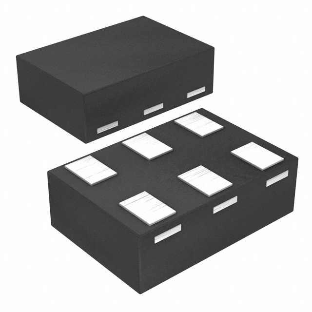
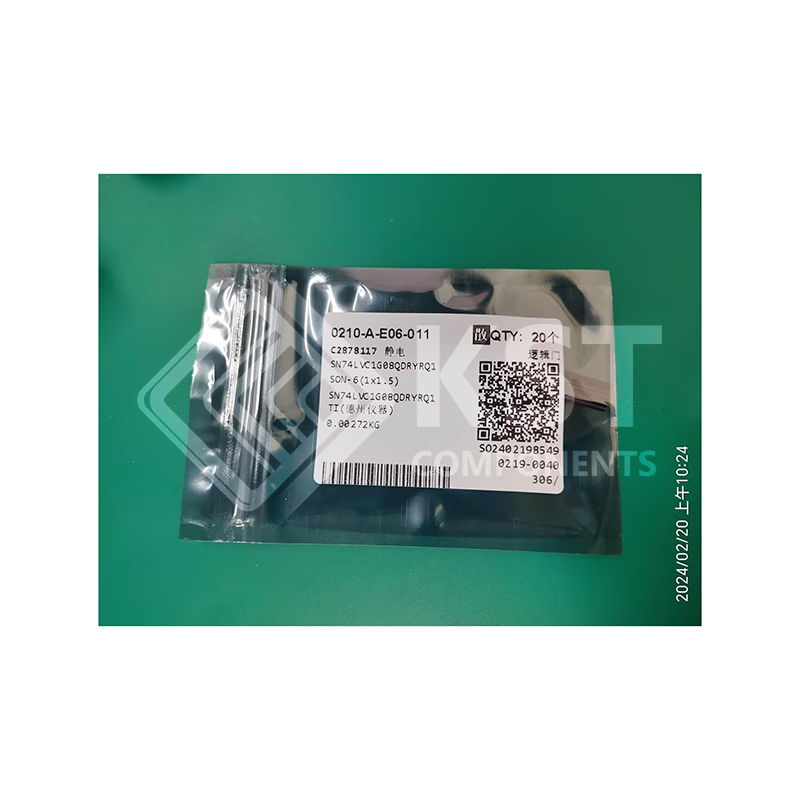
SN74LVC1G08QDRYRQ1

This single 2-input positive-AND gate is designed for
1.65-V to 5.5-V VCC operation.
The SN74LVC1G08-Q1 device performs the Boolean
function or in positive logic.
This device is fully specified for partial-power-down
applications using I off. The I off circuitry disables the
outputs, preventing damaging current backflow
through the device when it is powered down.
The CMOS device has high output drive while
maintaining low static power dissipation over a broad
VCC operating range.
The SN74LVC1G08 is available in a variety of
packages, including the small DRY package with a
body size of 1.45 mm × 1.00 mm.


Download Details PDF

Notice:

In stock will ship in 2 days. Real-time inventory pls confirm with us.

INQUIRY ONLINE


    SPECIFICATION

    • AEC-Q100 Qualified for Automotive Applications:
    – Device Temperature Grade 1: –40°C to
    +125°C, TA
    • Supports 5-V VCC Operation
    • Over-voltage Tolerant Inputs Accept Voltages to
    5.5 V
    • Provides Down Translation to VCC
    • Low Power Consumption, 10-μA Max ICC
    • ±24-mA Output Drive at 3.3 V
    • Ioff Supports Live Insertion, Partial-Power-Down
    Mode, and Back Drive Protection
    • Latch-Up Performance Exceeds 100 mA
    Per JESD 78, Class II
    • ESD Protection Exceeds JESD 22
    – 2000-V Human-Body Model (A114-A)
    – 200-V Machine Model (A115-A)
    – 1000-V Charged-Device Model (C101)