


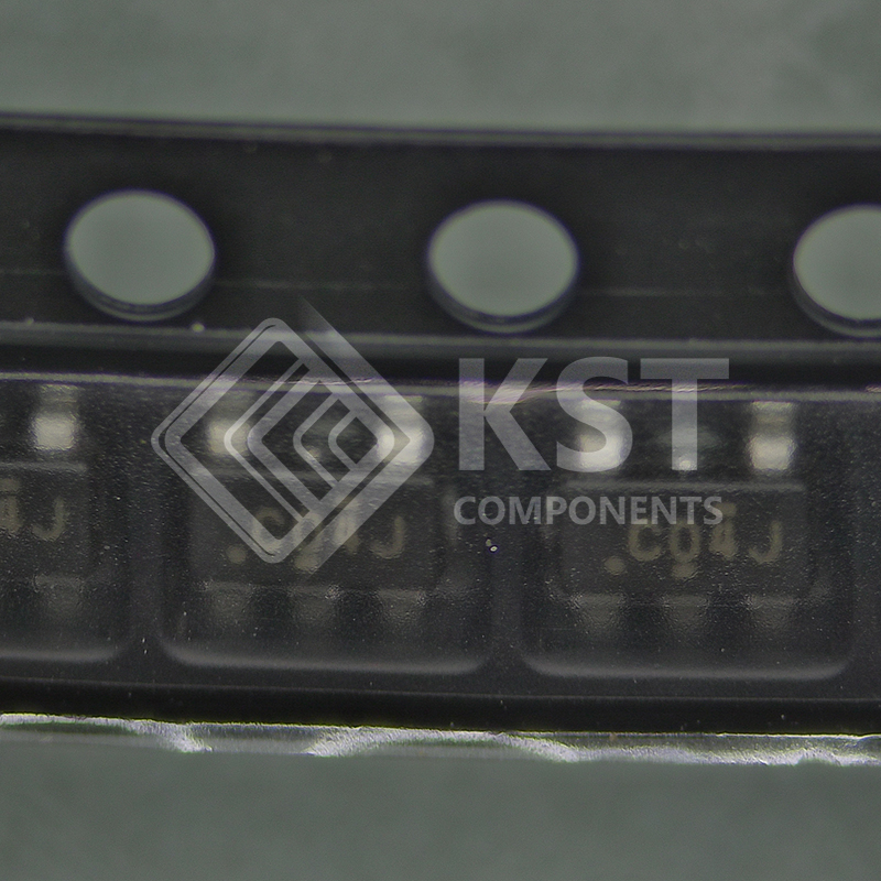

SN74LVC1G04DBVR
INQUIRY ONLINE
- Available in the Ultra-Small 0.64-mm2
Package (DPW) with 0.5-mm Pitch - Supports 5-V VCC Operation
- Inputs Accept Voltages up to 5.5 V Allowing Down Translation to VCC
- Max tpd of 3.3 ns at 3.3-V
- Low Power Consumption, 10-μA Max ICC
- ±24-mA Output Drive at 3.3-V
- Ioff Supports Live-Insertion, Partial-Power-Down Mode, and Back-Drive Protection
- Latch-Up Performance Exceeds 100 mA
Per JESD 78, Class II - ESD Protection Exceeds JESD 22
- 2000-V Human-Body Model (A114-A)
- 200-V Machine Model (A115-A)
- 1000-V Charged-Device Model (C101)