SN74AUP1T17DCKR

The SN74AUP1T17 performs the Boolean function Y = A with designation for logic-level translation applications with output referenced to supply VCC.

AUP technology is the industry–s lowest-power logic technology designed for use in extending battery-life in operating. All input levels that accept 1.8-V LVCMOS signals, while operating from either a single 3.3-V or 2.5-V VCC supply. This product also maintains excellent signal integrity.

The wide VCC range of 2.3 V to 3.6 V allows the possibility of switching output level to connect to external controllers or processors.

Schmitt-trigger inputs (ΔVT = 210 mV between positive and negative input transitions) offer improved noise immunity during switching transitions, which is especially useful on analog mixed-mode designs. Schmitt-trigger inputs reject input noise, ensure integrity of output signals, and allow for slow input signal transition.

Ioff is a feature that allows for powered-down conditions (VCC = 0 V) and is important in portable and mobile applications. When VCC = 0 V, signals in the range from 0 V to 3.6 V can be applied to the inputs and outputs of the device. No damage occurs to the device under these conditions.

The SN74AUP1T17 is designed with optimized current-drive capability of 4 mA to reduce line reflections, overshoot, and undershoot caused by high-drive outputs.

Category:

Download Details PDF

Notice:

In stock will ship in 2 days. Real-time inventory pls confirm with us.

INQUIRY ONLINE


    SPECIFICATION

    • Single-Supply Voltage Translator
    • Output Level Up to Supply VCC CMOS Level
      • 1.8 V to 3.3 V (at VCC = 3.3 V)
      • 2.5 V to 3.3 V (at VCC = 3.3 V)
      • 1.8 V to 2.5 V (at VCC = 2.5 V)
      • 3.3 V to 2.5 V (at VCC = 2.5 V
    • Schmitt-Trigger Inputs Reject Input Noise and
      Provide Better Output Signal Integrity
    • Ioff Supports Partial Power Down (VCC = 0 V)
    • Very Low Static Power Consumption:
      0.1 µA
    • Very Low Dynamic Power Consumption:
      0.9 µA
    • Latch-Up Performance Exceeds 100 mA Per
      JESD 78, Class II
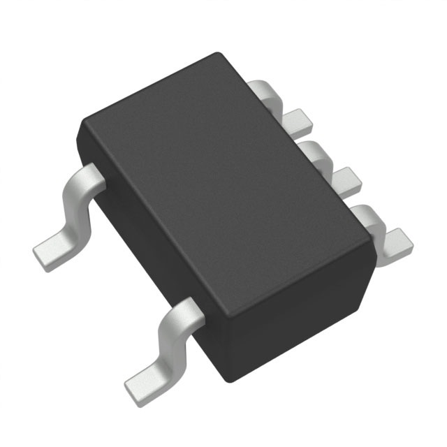
    • Pb-Free Packages Available: SC-70 (DCK)

      2 × 2.1 × 0.65 mm (Height 1.1 mm)

    • More Gate Options Available at
      www.ti.com/littlelogic
    • ESD Performance Tested Per JESD 22
      • 2000-V Human Body Model
        (A114-B, Class II)
      • 1000-V Charged-Device Model (C101)