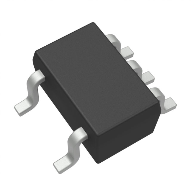
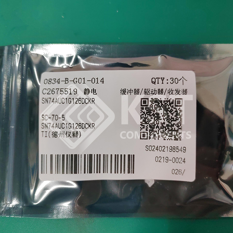
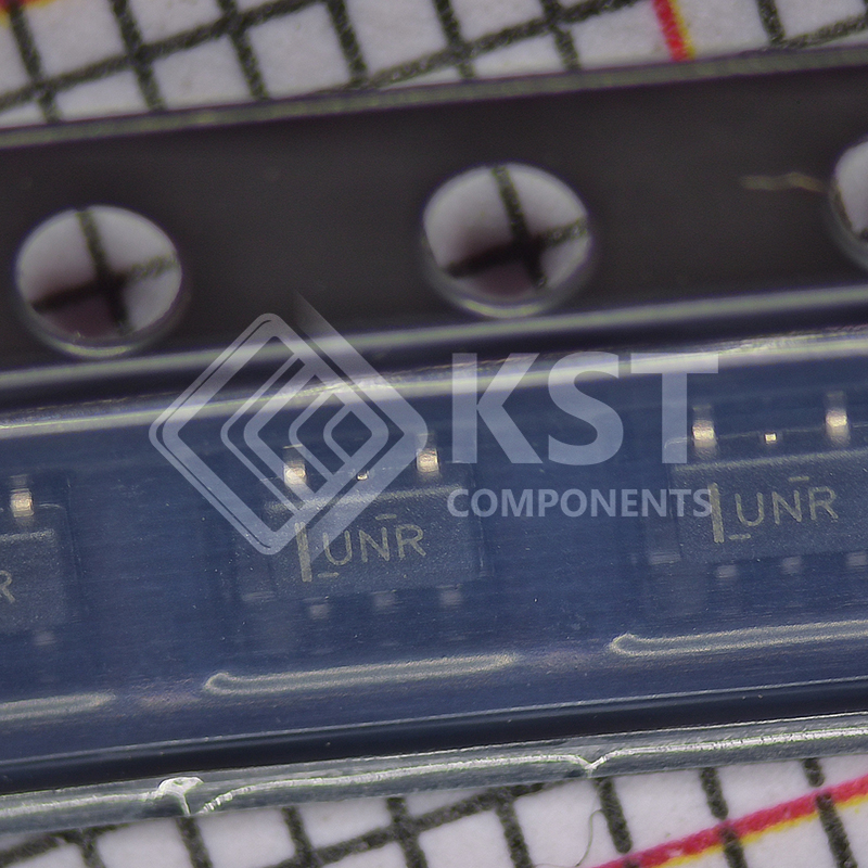
SN74AUC1G126DCKR

The SN74AUC1G126 bus buffer gate is operational
at 0.8-V to 2.7-V VCC, but is designed specifically for
1.65-V to 1.95-V VCC operation.
The SN74AUC1G126 device is a single line driver
with a tri-state output. The output is disabled when
the output-enable (OE) input is low.
To ensure the high-impedance state during power up
or power down, OE should be tied to GND through a
pulldown resistor; the minimum value of the resistor is
determined by the current-sourcing capability of the
driver.
NanoFree™ package technology is a major
breakthrough in device packaging concepts, using the
die as the package.
This device is fully specified for partial-power-down
applications using Ioff. The Ioff circuitry disables the
outputs, which prevents damaging current backflow
through the device when it is powered down.

Category:

Download Details PDF

Notice:

In stock will ship in 2 days. Real-time inventory pls confirm with us.

INQUIRY ONLINE


    SPECIFICATION

    • Latch-Up Performance Exceeds 100 mA Per
    JESD 78, Class II
    • ESD Protection Exceeds JESD22
    – 2000-V Human-Body Model (A114-A)
    – 200-V Machine Model (A115-A)
    – 1000-V Charged-Device Model (C101)
    • Available in TI’s NanoFree™ Package
    • Optimized for 1.8-V Operation and is 3.6-V I/O
    Tolerant to Support Mixed-Mode Signal Operation
    • Ioff Supports Partial Power Down Mode and Back
    Drive Protection
    • Sub-1 V Operable
    • Maximum tpd of 2.5 ns at 1.8 V
    • Low Power Consumption, 10-µA Maximum ICC
    • ±8-mA Output Drive at 1.8 V