


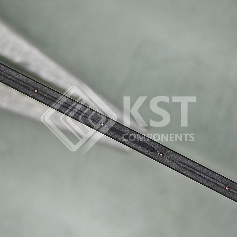
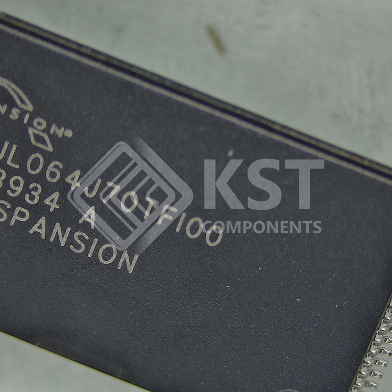
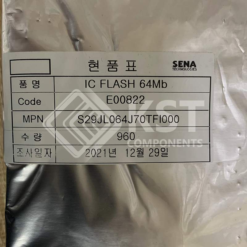
S29JL064J70TFI000
INQUIRY ONLINE
Simultaneous Read/Write operations
– Data can be continuously read from one bank while
executing erase/program functions in another bank
– Zero latency between read and write operations
Flexible bank architecture
– Read may occur in any of the three banks not being
programmed or erased
– Four banks may be grouped by customer to achieve
desired bank divisions
Boot sectors
– Top and bottom boot sectors in the same device
– Any combination of sectors can be erased
Manufactured on 0.11 µm Process Technology
Secured Silicon Region: Extra 256-byte sector
– Factory locked and identifiable: 16 bytes available for
secure, random factory Electronic Serial Number;
verifiable as factory locked through autoselect function
– Customer lockable: One-time programmable only. Once
locked, data cannot be changed
Zero power operation
– Sophisticated power management circuits reduce power
consumed during inactive periods to nearly zero
Compatible with JEDEC standards
– Pinout and software compatible with single-power-supply
flash standard
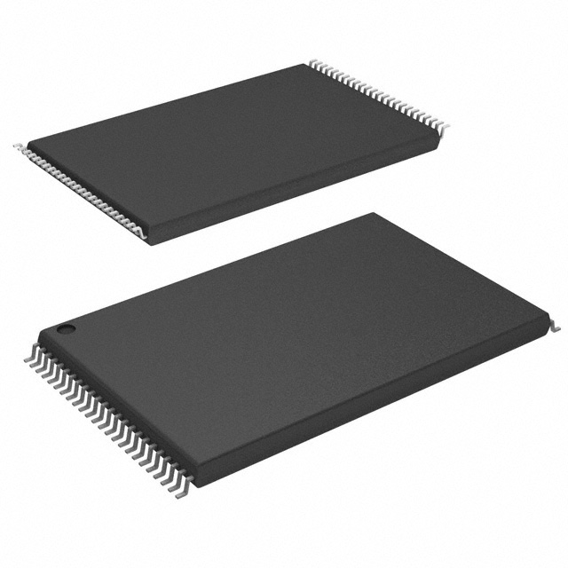
Package Options
48-ball Fine-pitch BGA
48-pin TSOP
Performance Characteristics
High performance
– Access time as fast as 55 ns
– Program time: 7 µs/word typical using accelerated
programming function
Ultra low power consumption (typical values)
– 2 mA active read current at 1 MHz
– 10 mA active read current at 5 MHz
– 200 nA in standby or automatic sleep mode
Cycling endurance: 1 million cycles per sector typical
Data retention: 20 years typical
Software Features
Supports Common Flash Memory Interface (CFI)
Erase suspend/erase resume
– Suspends erase operations to read data from, or program
data to, a sector that is not being erased, then resumes the
erase operation
Data# polling and toggle bits
– Provides a software method of detecting the status of
program or erase operations
Unlock bypass program command
– Reduces overall programming time when issuing multiple
program command sequences
Hardware Features
Ready/Busy# output (RY/BY#)
– Hardware method for detecting program or erase cycle
completion
Hardware reset pin (RESET#)
– Hardware method of resetting the internal state machine to
the read mode
WP#/ACC input pin
– Write protect (WP#) function protects sectors 0, 1, 140,
and 141, regardless of sector protect status
– Acceleration (ACC) function accelerates program timing
Sector Protection
– Hardware method to prevent any program or erase
operation within a sector
– Temporary Sector Unprotect allows changing data in
protected sectors in-system