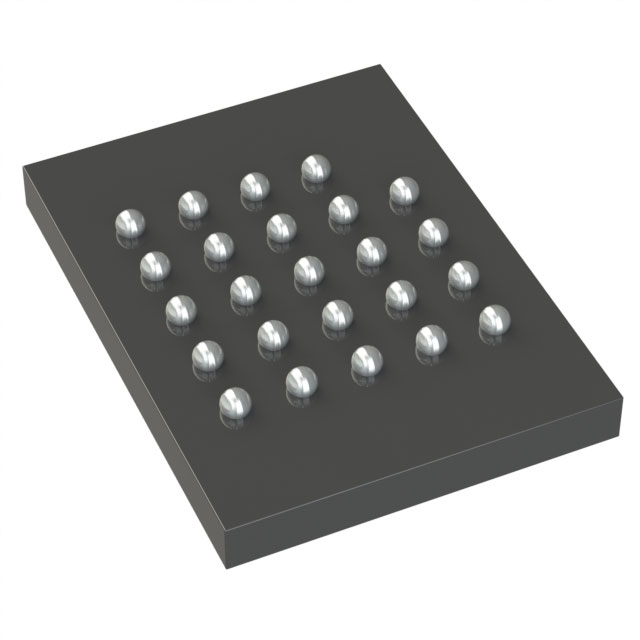
S26KL512SDABHB020

The HYPERFLASH™ family of products are high-speed CMOS, MIRRORBIT™ NOR flash devices with the
HYPERBUS™ low signal count DDR interface, that achieves high speed read throughput. The DDR protocol
transfers two data bytes per clock cycle on the data (DQ) signals. A read or write access for the HYPERFLASH™
consists of a series of 16-bit wide, one clock cycle data transfers at the internal HYPERFLASH™ core and two
corresponding 8-bit wide, one-half-clock-cycle data transfers on the DQ signals.
Both data and command/address information are transferred in DDR fashion over the 8-bit data bus. The clock
input signals are used for signal capture by the HYPERFLASH™ device when receiving command/address/data
information on the DQ signals. The read data strobe (RWDS) is an output from the HYPERFLASH™ device that
indicates when data is being transferred from the memory to the host. RWDS is referenced to the rising and falling
edges of CK during the data transfer portion of read operations.
Command/address/write-data values are center aligned with the clock edges and read-data values are edge
aligned with the transitions of RWDS.
Read and write operations to the HYPERFLASH™ device are burst oriented. Read transactions can be specified to
use either a wrapped or linear burst. During wrapped operation, accesses start at a selected location and
continue for a configured number of locations in a group wrap sequence. During linear operation accesses start
at a selected location and continue in a sequential manner until the read operation is terminated, when CS#
returns HIGH. Write transactions transfer one or more 16-bit values.

Category:

Download Details PDF

Notice:

In stock will ship in 2 days. Real-time inventory pls confirm with us.

INQUIRY ONLINE


    SPECIFICATION

    • 3.0 V I/O, 11 bus signals
    – Single ended clock
    • 1.8 V I/O, 12 bus signals
    – Differential clock (CK, CK#)
    • Chip Select (CS#)
    • 8-bit data bus (DQ[7:0])
    • Read-write data strobe (RWDS)
    – HYPERFLASH™ memories use RWDS only as a Read Data Strobe
    • Up to 333-MBps sustained read throughput
    • DDR: two data transfers per clock
    • 166-MHz clock rate (333 MBps) at 1.8 V VCC
    • 100-MHz clock rate (200 MBps) at 3.0 V VCC
    • 96-ns initial random read access time
    – Initial random access read latency: 5 to 16 clock cycles
    • Sequential burst transactions
    • Configurable burst characteristics
    – Wrapped burst lengths:
    • 16 bytes (8 clocks)
    • 32 bytes (16 clocks)
    • 64 bytes (32 clocks)
    – Linear burst
    – Hybrid option: one wrapped burst followed by linear burst
    – Wrapped or linear burst type selected in each transaction
    – Configurable output drive strength
    • Low power modes
    – Active clock stop during read: 12 mA, no wake-up required
    – Standby: 25 µA (typical), no wake-up required
    – Deep Power-Down: 8 µA (typical)
    • 300 µs wake-up required
    • INT# output to generate external interrupt
    – Busy to Ready transition
    – ECC detection
    • RSTO# output to generate system level power-on reset
    – User configurable RSTO# LOW period
    • 512-byte program buffer

    • Sector erase
    – Uniform 256-KB sectors
    – Optional eight 4-KB parameter sectors (32 KB total)
    • Advanced sector protection
    – Volatile and non-volatile protection methods for each sector
    • Separate 1024-byte one-time program array
    • Operating temperature
    – Industrial (–40°C to +85°C)
    – Industrial Plus (–40°C to +105°C)
    – Extended (–40°C to +125°C)
    – Automotive, AEC-Q100 grade 3 (–40°C to +85°C)
    – Automotive, AEC-Q100 grade 2 (–40°C to +105°C)
    – Automotive, AEC-Q100 grade 1 (–40°C to +125°C)
    • ISO/TS16949 and AEC Q100 Certified
    • Endurance
    – 100,000 program/erase cycles
    • Retention
    – 20 year data retention
    • Erase and program current
    – Max peak < 100 mA
    • Packaging options
    – 24-ball FBGA
    • Additional features
    – ECC 1-bit correction, 2-bit detection
    – CRC