


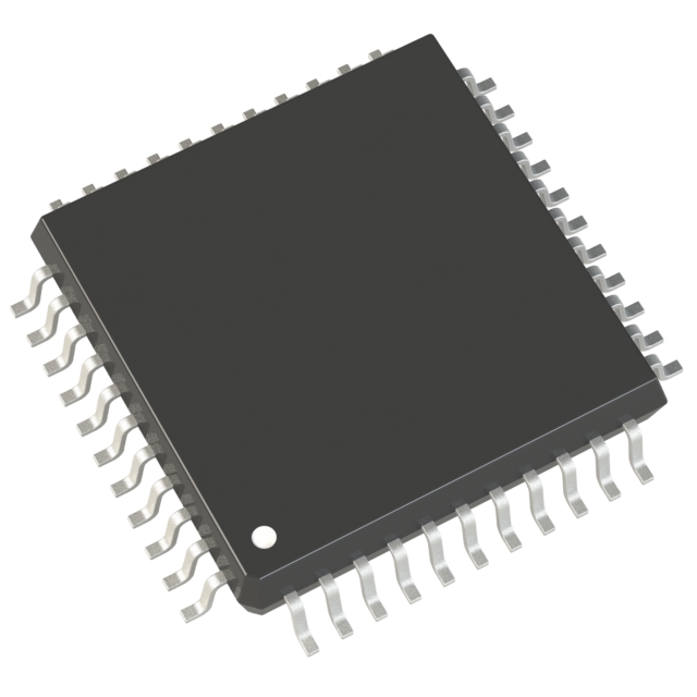
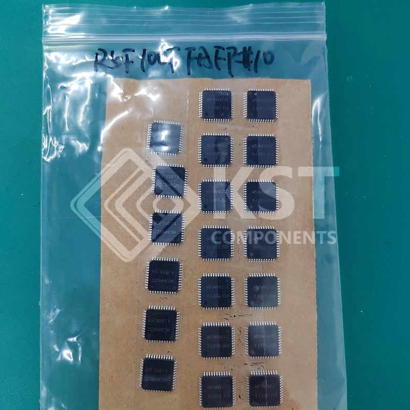
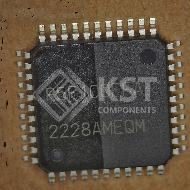
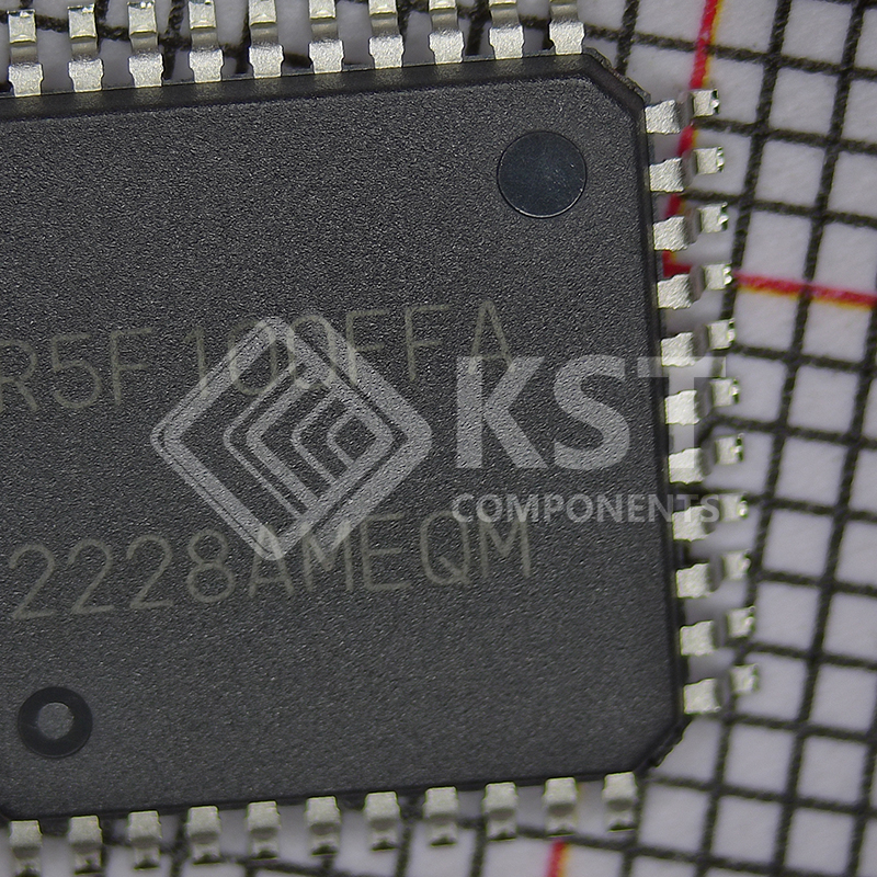

R5F100FFAFP#10
INQUIRY ONLINE
Ultra-low power consumption technology
VDD = single power supply voltage of 1.6 to 5.5 V
HALT mode
STOP mode
SNOOZE mode
RL78 CPU core
CISC architecture with 3-stage pipeline
Minimum instruction execution time: Can be changed
from high speed (0.03125 μs: @ 32 MHz operation
with high-speed on-chip oscillator) to ultra-low speed
(30.5 μs: @ 32.768 kHz operation with subsystem
clock)
Address space: 1 MB
General-purpose registers: (8-bit register × 8) × 4
banks
On-chip RAM: 2 to 32 KB
Code flash memory
Code flash memory: 16 to 512 KB
Block size: 1 KB
Prohibition of block erase and rewriting (security
function)
On-chip debug function
Self-programming (with boot swap function/flash shield
window function)
Data Flash Memory
Data flash memory: 4 KB to 8 KB
Back ground operation (BGO): Instructions can be
executed from the program memory while rewriting the
data flash memory.
Number of rewrites: 1,000,000 times (TYP.)
Voltage of rewrites: VDD = 1.8 to 5.5 V
High-speed on-chip oscillator
Select from 32 MHz, 24 MHz, 16 MHz, 12 MHz, 8 MHz,
6 MHz, 4 MHz, 3 MHz, 2 MHz, and 1 MHz
High accuracy: +/- 1.0 % (VDD = 1.8 to 5.5 V, TA = -20
to +85°C)
Operating ambient temperature
TA = -40 to +85°C (A: Consumer applications, D:
Industrial applications )
TA = -40 to +105°C (G: Industrial applications)
Power management and reset function
On-chip power-on-reset (POR) circuit
On-chip voltage detector (LVD) (Select interrupt and
reset from 14 levels)
DMA (Direct Memory Access) controller
2/4 channels
Number of clocks during transfer between 8/16-bit
SFR and internal RAM: 2 clocks
Multiplier and divider/multiply-accumulator
16 bits × 16 bits = 32 bits (Unsigned or signed)
32 bits ÷ 32 bits = 32 bits (Unsigned)
16 bits × 16 bits + 32 bits = 32 bits (Unsigned or
signed)
Serial interface
Simplified SPI (CSI Note 1): 2 to 8 channels
UART/UART (LIN-bus supported): 2 to 4 channels
I2C/Simplified I2C communication: 3 to 10 channels
Timer
16-bit timer: 8 to 16 channels
12-bit interval timer: 1 channel
Real-time clock: 1 channel (calendar for 99 years,
alarm function, and clock
correction function)
Watchdog timer: 1 channel (operable with the
dedicated low-speed on-chip
oscillator)
A/D converter
8/10-bit resolution A/D converter (VDD = 1.6 to 5.5 V)
Analog input: 6 to 26 channels
Internal reference voltage (1.45 V) and temperature
sensor Note 2
I/O port
I/O port: 16 to 120 (N-ch open drain I/O [withstand
voltage of 6 V]: 0 to 4, N-ch open drain I/O
[VDD withstand voltage Note 3/EVDD withstand
voltage Note 4]: 5 to 25)
Can be set to N-ch open drain, TTL input buffer, and
on-chip pull-up resistor
Different potential interface: Can connect to a 1.8/2.5/3
V device
On-chip key interrupt function
On-chip clock output/buzzer output controller
Others
On-chip BCD (binary-coded decimal) correction circuit