


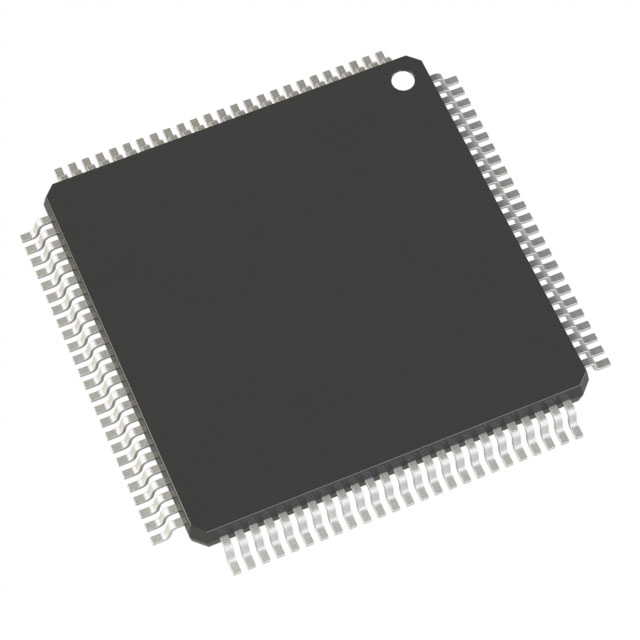
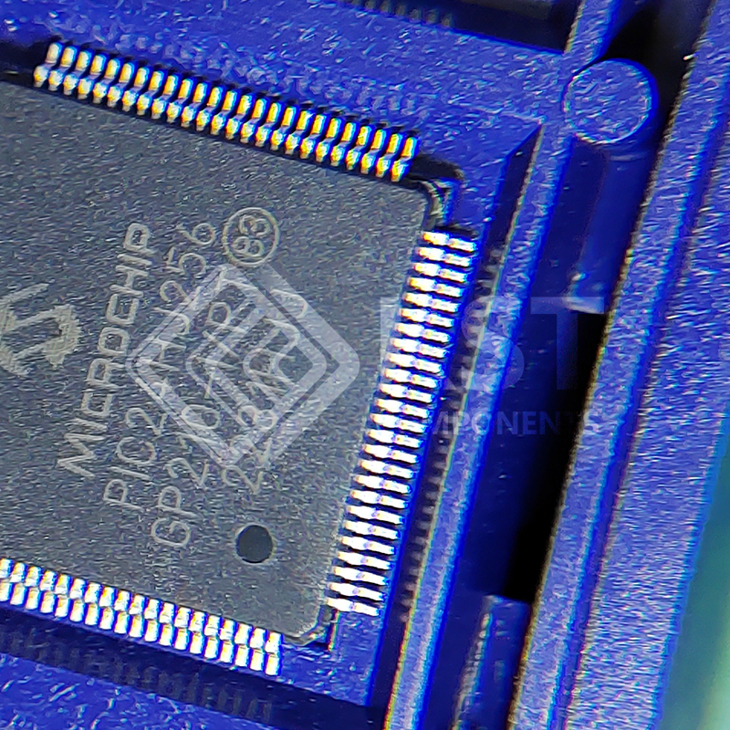
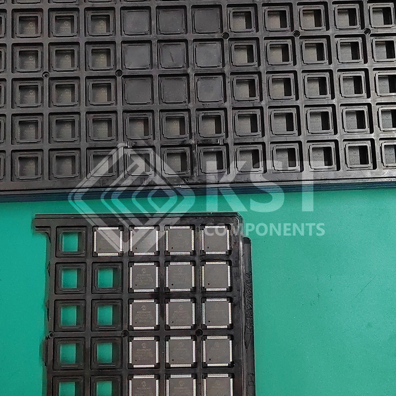
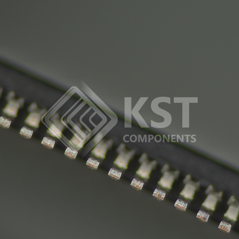
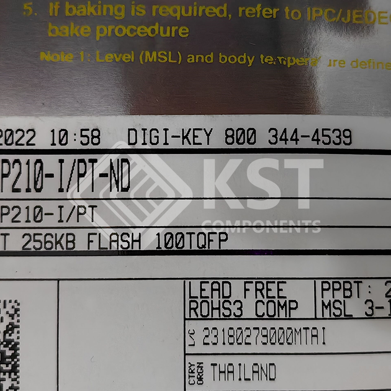
PIC24HJ256GP210-I/PT
INQUIRY ONLINE
Operating Range:
• Up to 40 MIPS operation (at 3.0-3.6V):
– Industrial temperature range
(-40°C to +85°C)
High-Performance CPU:
• Modified Harvard architecture
• C compiler optimized instruction set
• 16-bit wide data path
• 24-bit wide instructions
• Linear program memory addressing up to 4M
instruction words
• Linear data memory addressing up to 64 Kbytes
• 71 base instructions: mostly 1 word/1 cycle
• Sixteen 16-bit General Purpose Registers
• Flexible and powerful Indirect Addressing modes
• Software stack
• 16 x 16 multiply operations
• 32/16 and 16/16 divide operations
• Up to ±16-bit data shifts
Direct Memory Access (DMA):
• 8-channel hardware DMA
• 2 Kbytes dual ported DMA buffer area
(DMA RAM) to store data transferred via DMA:
– Allows data transfer between RAM and a
peripheral while CPU is executing code
(no cycle stealing)
• Most peripherals support DMA
Interrupt Controller:
• 5-cycle latency
• Up to 61 available interrupt sources
• Up to five external interrupts
• Seven programmable priority levels
• FIve processor exceptions
Digital I/O:
• Up to 85 programmable digital I/O pins
• Wake-up/Interrupt-on-Change on up to 24 pins
• Output pins can drive from 3.0V to 3.6V
• All digital input pins are 5V tolerant
• 4 mA sink on all I/O pins
On-Chip Flash and SRAM:
• Flash program memory, up to 256 Kbytes
• Data SRAM, up to 16 Kbytes (includes 2 Kbytes
of DMA RAM)
System Management:
• Flexible clock options:
– External, crystal, resonator, internal RC
– Fully integrated PLL
– Extremely low jitter PLL
• Power-up Timer
• Oscillator Start-up Timer/Stabilizer
• Watchdog Timer with its own RC oscillator
• Fail-Safe Clock Monitor
• Reset by multiple sources
Power Management:
• On-chip 2.5V voltage regulator
• Switch between clock sources in real time
• Idle, Sleep and Doze modes with fast wake-up
Timers/Capture/Compare/PWM:
• Timer/Counters, up to nine 16-bit timers:
– Can pair up to make four 32-bit timers
– One timer runs as Real-Time Clock with
external 32.768 kHz oscillator
– Programmable prescaler
• Input Capture (up to eight channels):
– Capture on up, down or both edges
– 16-bit capture input functions
– 4-deep FIFO on each capture
• Output Compare (up to eight channels):
– Single or Dual 16-Bit Compare mode
– 16-bit Glitchless PWM mode
Communication Modules:
• 3-wire SPI (up to two modules):
– Framing supports I/O interface to simple
codecs
– Supports 8-bit and 16-bit data
– Supports all serial clock formats and
sampling modes
• I2C™ (up to two modules):
– Full Multi-Master Slave mode support
– 7-bit and 10-bit addressing
– Bus collision detection and arbitration
– Integrated signal conditioning
– Slave address masking
• UART (up to two modules):
– Interrupt on address bit detect
– Interrupt on UART error
– Wake-up on Start bit from Sleep mode
– 4-character TX and RX FIFO buffers
– LIN bus support
– IrDA® encoding and decoding in hardware
– High-Speed Baud mode
– Hardware Flow Control with CTS and RTS
• Enhanced CAN (ECAN™ module) 2.0B active
(up to two modules):
– Up to eight transmit and up to 32 receive buffers
– 16 receive filters and 3 masks
– Loopback, Listen Only and Listen All
Messages modes for diagnostics and bus
monitoring
– Wake-up on CAN message
– Automatic processing of Remote
Transmission Requests
– FIFO mode using DMA
– DeviceNet™ addressing support
Analog-to-Digital Converters:
• Up to two Analog-to-Digital Converter (ADC)
modules in a device
• 10-bit, 1.1 Msps or 12-bit, 500 ksps conversion:
– Two, four, or eight simultaneous samples
– Up to 32 input channels with auto-scanning
– Conversion start can be manual or
synchronized with one of four trigger sources
– Conversion possible in Sleep mode
– ±1 LSb max integral nonlinearity
– ±1 LSb max differential nonlinearity
CMOS Flash Technology:
• Low-power, high-speed Flash technology
• Fully static design
• 3.3V (±10%) operating voltage
• Industrial temperature
• Low-power consumption
Packaging:
• 100-pin TQFP (14x14x1 mm and 12x12x1 mm)
• 64-pin TQFP (10x10x1 mm)