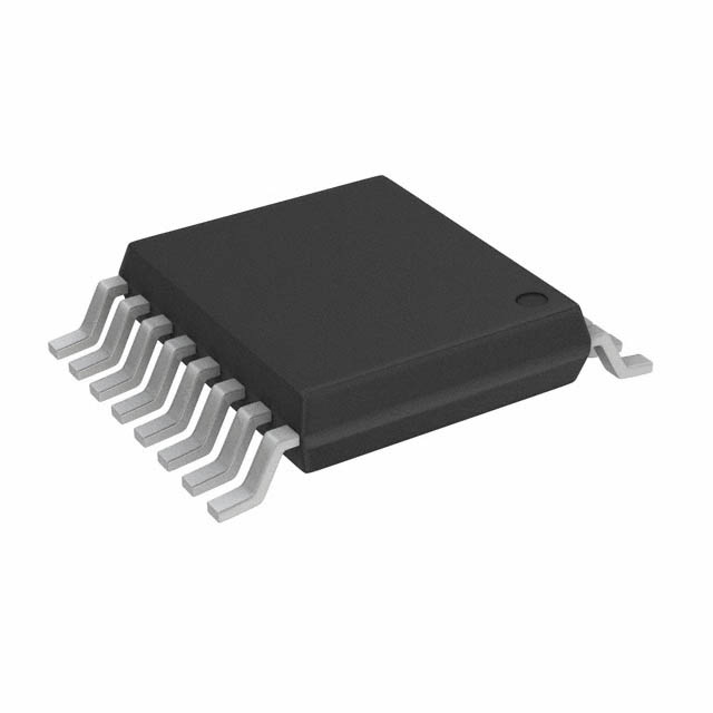
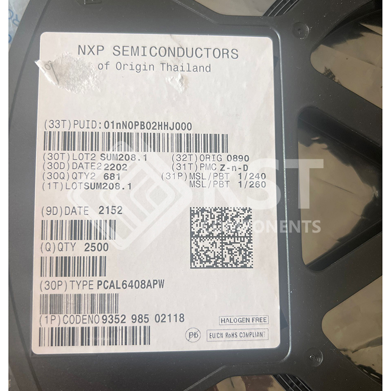
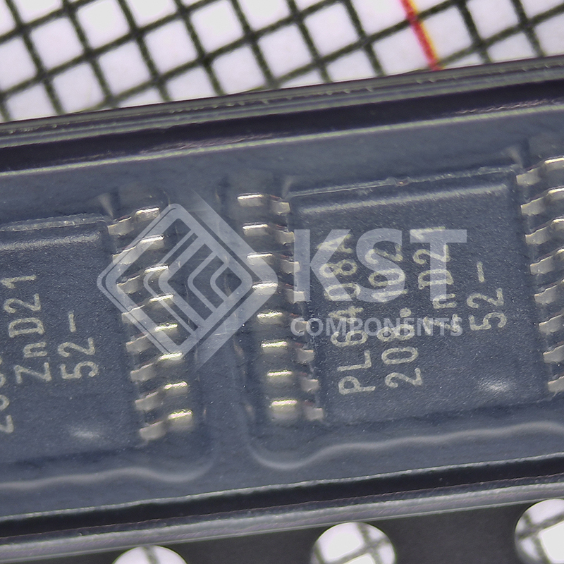
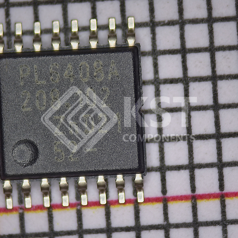
PCAL6408APWJ

The PCAL6408A is an 8-bit general-purpose I/O expander that provides remote I/O expansion for most microcontroller families via the I2C-bus interface.
NXP I/O expanders provide a simple solution when additional I/Os are needed while keeping interconnections to a minimum, for example, in battery-powered mobile applications for interfacing to sensors, push buttons, keypad, etc. In addition to providing a flexible set of GPIOs, it simplifies interconnection of a processor running at one voltage level to I/O devices operating at a different (usually higher) voltage level. The PCAL6408A has built-in level shifting feature that makes these devices extremely flexible in mixed signal environments where communication between incompatible I/O voltages is required. Its wide VDD range of 1.65 V to 5.5 V on the dual power rail allows seamless communications with next-generation low voltage microprocessors and microcontrollers on the interface side (SDA/SCL) and peripherals at a higher voltage on the port side. There are two supply voltages for PCAL6408A: VDD(I2C-bus) and VDD(P). VDD(I2C-bus) provides the supply voltage for the interface at the master side (for example, a microcontroller) and the VDD(P) provides the supply for core circuits and Port P. The bidirectional voltage level translation in the PCAL6408A is provided through VDD(I2C-bus). VDD(I2C-bus) should be connected to the VDD of the external SCL/SDA lines. This indicates the VDD level of the I2C-bus to the PCAL6408A, while the voltage level on Port P of the PCAL6408A is determined by the VDD(P). The PCAL6408A contains the PCA6408A register set of 8-bit Configuration, Input, Output, and Polarity Inversion registers and additionally, the PCAL6408A has Agile I/O, which are additional features specifically designed to enhance the I/O. These additional features are: programmable output drive strength, latchable inputs, programmable
pull-up/pull-down resistors, maskable interrupt, interrupt status register, programmable open-drain or push-pull outputs. The PCAL6408A is a pin-to-pin replacement to the PCA6408A, however, the PCAL6408A powers up with all I/O interrupts masked. This mask default allows for a board bring-up free of spurious interrupts at power-up.
At power-on, the I/Os are configured as inputs. However, the system master can enable the I/Os as either inputs or outputs by writing to the I/O configuration bits. The data for each input or output is kept in the corresponding input or output register. The polarity of the Input Port register can be inverted with the Polarity Inversion register, saving external logic gates. Programmable pull-up and pull-down resistors eliminate the need for discrete components.

The system master can reset the PCAL6408A in the event of a time-out or other improper operation by asserting a LOW in the RESET input. The power-on reset puts the registers
in their default state and initializes the I2C-bus/SMBus state machine. The RESET pin causes the same reset/initialization to occur without de-powering the part. The PCAL6408A open-drain interrupt (INT) output is activated when any input state differs from its corresponding Input Port register state and is used to indicate to the system master that an input state has changed. INT can be connected to the interrupt input of a microcontroller. By sending an interrupt signal on this line, the remote I/O can inform the microcontroller if there is incoming data on its ports without having to communicate via the I2C-bus. Thus, the PCAL6408A can remain a simple slave device. The input latch feature holds or latches the input pin state and keeps the logic values that created the interrupt until the master can service the interrupt. This minimizes the host’s interrupt service response for fast moving inputs. The device Port P outputs have 25 mA sink capabilities for directly driving LEDs while consuming low device current.
One hardware pin (ADDR) can be used to program and vary the fixed I2C-bus address and allow up to two devices to share the same I2C-bus or SMBus.


Download Details PDF

Notice:

In stock will ship in 2 days. Real-time inventory pls confirm with us.

INQUIRY ONLINE


    SPECIFICATION

     I2C-bus to parallel port expander
     Operating power supply voltage range of 1.65 V to 5.5 V
     Allows bidirectional voltage-level translation and GPIO expansion between:
     1.8 V SCL/SDA and 1.8 V, 2.5 V, 3.3 V or 5 V Port P
     2.5 V SCL/SDA and 1.8 V, 2.5 V, 3.3 V or 5 V Port P
     3.3 V SCL/SDA and 1.8 V, 2.5 V, 3.3 V or 5 V Port P
     5 V SCL/SDA and 1.8 V, 2.5 V, 3.3 V or 5 V Port P
     Low standby current consumption of 1 A
     Schmitt-trigger action allows slow input transition and better switching noise immunity
    at the SCL and SDA inputs
     Vhys = 0.18 V (typical) at 1.8 V
     Vhys = 0.25 V (typical) at 2.5 V
     Vhys = 0.33 V (typical) at 3.3 V
     Vhys = 0.5 V (typical) at 5 V
     5 V tolerant I/O ports
     Active LOW reset input (RESET)
     Open-drain active LOW interrupt output (INT)
     400 kHz Fast-mode I2C-bus
     Internal power-on reset
     Power-up with all channels configured as inputs
     No glitch on power-up
     Noise filter on SCL/SDA inputs
     Latched outputs with 25 mA drive maximum capability for directly driving LEDs
     Latch-up performance exceeds 100 mA per JESD 78, Class II

     ESD protection exceeds JESD 22
     2000 V Human-Body Model (A114-A)
     1000 V Charged-Device Model (C101)
     Packages offered: HVQFN16, TSSOP16, XQFN16,
    XFBGA16 (1.6 mm  1.6 mm  0.5 mm), X2QFN16 (LGA, Land Grid Array) 1.6 mm x
    1.6 mm x 0.35 mm