PCA9515ADP

The PCA9515A is a CMOS integrated circuit intended for application in I2C-bus and
SMBus systems.
While retaining all the operating modes and features of the I2C-bus system, it permits
extension of the I2C-bus by buffering both the data (SDA) and the clock (SCL) lines, thus
enabling two buses of 400 pF.
The I2C-bus capacitance limit of 400 pF restricts the number of devices and bus length.
Using the PCA9515A enables the system designer to isolate two halves of a bus, thus
more devices or longer length can be accommodated. It can also be used to run two
buses, one at 5 V and the other at 3.3 V or a 400 kHz and 100 kHz bus, where the
100 kHz bus is isolated when 400 kHz operation of the other is required.
Two or more PCA9515As cannot be put in series. The PCA9515A design does not
allow this configuration. Since there is no direction pin, slightly different ‘legal’ low voltage
levels are used to avoid lock-up conditions between the input and the output. A ‘regular
LOW’ applied at the input of a PCA9515A will be propagated as a ‘buffered LOW’ with a
slightly higher value. When this ‘buffered LOW’ is applied to another PCA9515A,
PCA9516A or PCA9518/A in series, the second PCA9515A, PCA9516A or PCA9518/A
will not recognize it as a ‘regular LOW’ and will not propagate it as a ‘buffered LOW’ again.
The PCA9510/A, PCA9511/A, PCA9512/A, PCA9513/A, PCA9514/A cannot be used in
series with the PCA9515A, PCA9516A or PCA9518/A, but can be used in series with
themselves since they use shifting instead of static offsets to avoid lock-up conditions.
The output pull-down of each internal buffer is set for approximately 0.5 V, while the input
threshold of each internal buffer is set about 0.07 V lower, when the output is internally
driven LOW. This prevents a lock-up condition from occurring.

Category:

Download Details PDF

Notice:

In stock will ship in 2 days. Real-time inventory pls confirm with us.

INQUIRY ONLINE


    SPECIFICATION

     2-channel, bidirectional buffer
     I
    2C-bus and SMBus compatible
     Active HIGH repeater enable input
     Open-drain input/outputs
     Lock-up free operation
     Supports arbitration and clock stretching across the repeater
     Accommodates Standard-mode and Fast-mode I2C-bus devices and multiple masters
     Powered-off high-impedance I2C-bus pins
     Operating supply voltage range of 2.3 V to 3.6 V
     5.5 V tolerant I2C-bus and enable pins

     0 Hz to 400 kHz clock frequency (the maximum system operating frequency may be
    less than 400 kHz because of the delays added by the repeater)
     ESD protection exceeds 2000 V HBM per JESD22-A114 and 1000 V CDM per
    JESD22-C101
     Latch-up testing is done to JEDEC Standard JESD78 which exceeds 100 mA
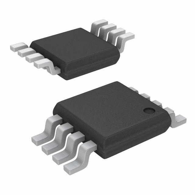
     Packages offered: SO8, TSSOP8 (MSOP8), HWSON8