PCA9306GF,115

The PCA9306 is a dual bidirectional I2C-bus and SMBus voltage-level translator with an enable (EN) input, and
is operational from 1.0 V to 3.6 V (Vref(1)) and 1.8 V to 5.5 V (Vbias(ref)(2)).
The PCA9306 allows bidirectional voltage translations between 1.0 V and 5 V without the use of a direction pin.
The low ON-state resistance (Ron) of the switch allows connections to be made with minimal propagation delay.
When EN is HIGH, the translator switch is on, and the SCL1 and SDA1 I/O are connected to the SCL2 and
SDA2 I/O, respectively, allowing bidirectional data flow between ports. When EN is LOW, the translator switch is
off, and a high-impedance state exists between ports.
The PCA9306 is not a bus buffer like the PCA9509 or PCA9517A that provide both level translation and
physically isolate the capacitance to either side of the bus when both sides are connected. The PCA9306 only
isolates both sides when the device is disabled and provides voltage level translation when active.
The PCA9306 can also be used to run two buses, one at 400 kHz operating frequency and the other at 100 kHz
operating frequency. If the two buses are operating at different frequencies, the 100 kHz bus must be isolated
when the 400 kHz operation of the other bus is required. If the controller is running at 400 kHz, the maximum
system operating frequency may be less than 400 kHz because of the delays added by the translator.
As with the standard I2C-bus system, pull-up resistors are required to provide the logic HIGH levels on the
translator’s bus. The PCA9306 has a standard open-collector configuration of the I2C-bus. The size of these
pull-up resistors depends on the system, but each side of the translator must have a pull-up resistor. The device
is designed to work with Standard-mode, Fast-mode and Fast-mode Plus I2C-bus devices in addition to SMBus
devices. The maximum frequency is dependent on the RC time constant, but generally supports > 2 MHz.
When the SDA1 or SDA2 port is LOW, the clamp is in the ON-state and a low resistance connection exists
between the SDA1 and SDA2 ports. Assuming the higher voltage is on the SDA2 port when the SDA2 port is
HIGH, the voltage on the SDA1 port is limited to the voltage set by VREF1. When the SDA1 port is HIGH, the
SDA2 port is pulled to the drain pull-up supply voltage (Vpu(D)) by the pull-up resistors. This functionality allows
a seamless translation between higher and lower voltages selected by the user without the need for directional
control. The SCL1/SCL2 channel also functions as the SDA1/SDA2 channel.
All channels have the same electrical characteristics and there is minimal deviation from one output to another
in voltage or propagation delay. This is a benefit over discrete transistor voltage translation solutions, since
the fabrication of the switch is symmetrical. The translator provides excellent ESD protection to lower voltage
devices, and at the same time protects less ESD-resistant devices.

Category:

Download Details PDF

Notice:

In stock will ship in 2 days. Real-time inventory pls confirm with us.

INQUIRY ONLINE


    SPECIFICATION

    • 2-bit bidirectional translator for SDA and SCL lines in mixed-mode I2C-bus applications
    • Standard-mode, Fast-mode, and Fast-mode Plus I2C-bus and SMBus compatible

    • Less than 1.5 ns maximum propagation delay to accommodate Standard-mode and Fast-mode I2C-bus
    devices and multiple controllers
    • Allows voltage level translation between:
    – 1.0 V Vref(1) and 1.8 V, 2.5 V, 3.3 V or 5 V Vbias(ref)(2)
    – 1.2 V Vref(1) and 1.8 V, 2.5 V, 3.3 V or 5 V Vbias(ref)(2)
    – 1.8 V Vref(1) and 3.3 V or 5 V Vbias(ref)(2)
    – 2.5 V Vref(1) and 5 V Vbias(ref)(2)
    – 3.3 V Vref(1) and 5 V Vbias(ref)(2)
    • Provides bidirectional voltage translation with no direction pin
    • Low 3.5 Ω ON-state connection between input and output ports provides less signal distortion
    • Open-drain I2C-bus I/O ports (SCL1, SDA1, SCL2 and SDA2)
    • 5 V tolerant I2C-bus I/O ports to support mixed-mode signal operation
    • High-impedance SCL1, SDA1, SCL2 and SDA2 pins for EN = LOW
    • Lock-up free operation
    • Flow through pinout for ease of printed-circuit board trace routing
    • ESD protection exceeds 2000 V HBM per JESD22-A114 and 1000 V CDM per JESD22-C101
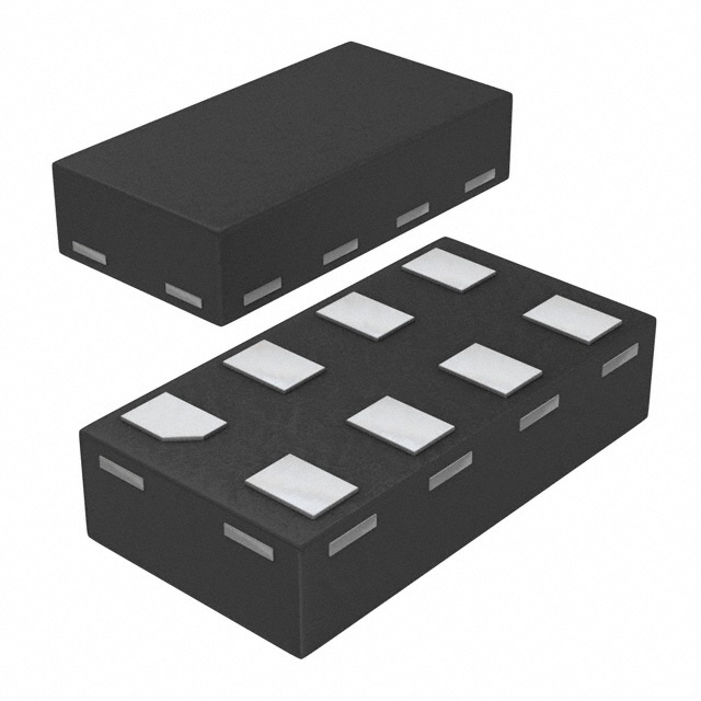
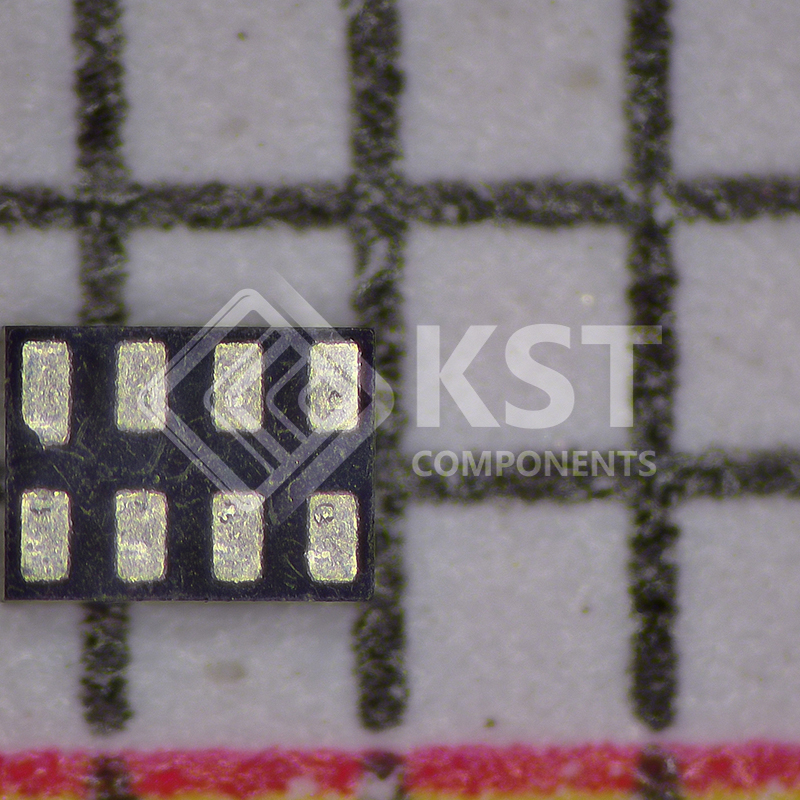
    • Packages offered: SO8, TSSOP8, VSSOP8, XQFN8, XSON8, X2SON8