


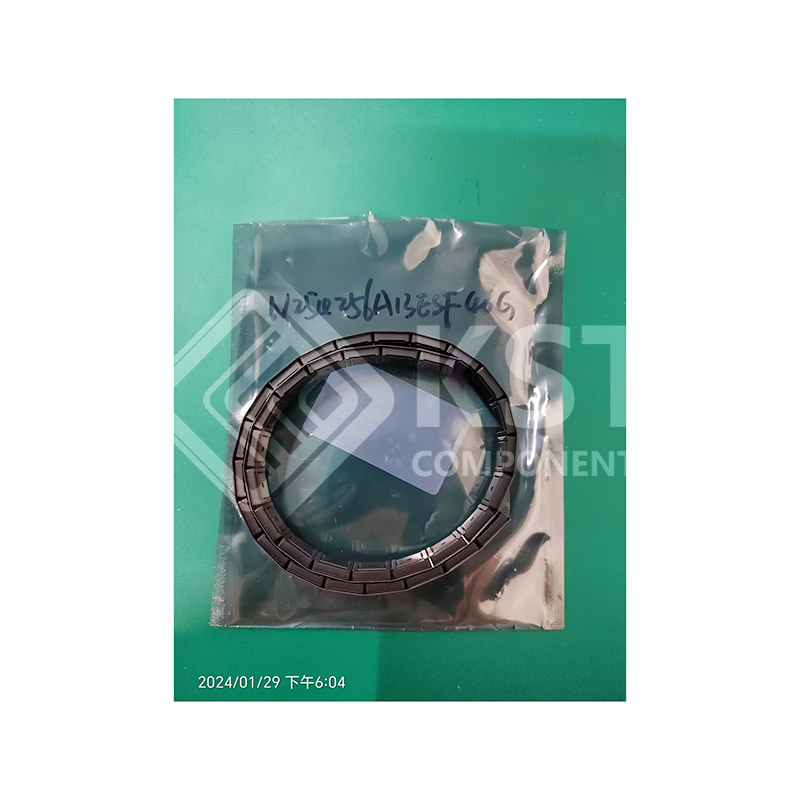


N25Q256A13ESF40G
INQUIRY ONLINE
• SPI-compatible serial bus interface
• Double transfer rate (DTR) mode
• 2.7–3.6V single supply voltage
• 108 MHz (MAX) clock frequency supported for all
protocols in single transfer rate (STR) mode
• 54 MHz (MAX) clock frequency supported for all
protocols in DTR mode
• Dual/quad I/O instruction provides increased
throughput up to 54 MB/s
• Supported protocols
– Extended SPI, dual I/O, and quad I/O
– DTR mode supported on all
• Execute-in-place (XIP) mode for all three protocols
– Configurable via volatile or nonvolatile registers
– Enables memory to work in XIP mode directly after power-on
• PROGRAM/ERASE SUSPEND operations
• Continuous read of entire memory via a single command
– Fast read
– Quad or dual output fast read
– Quad or dual I/O fast read
• Flexible to fit application
– Configurable number of dummy cycles
– Output buffer configurable
• Software reset
• 3-byte and 4-byte addressability mode supported
• 64-byte, user-lockable, one-time programmable
(OTP) dedicated area
• An additional reset pin is available on the following
devices
– N25Q256A83ESF40x, N25Q256A83E1240x
• Erase capability
– Subsector erase 4KB uniform granularity blocks
– Sector erase 64KB uniform granularity blocks
– Full-chip erase
• Write protection
– Software write protection applicable to every
64KB sector via volatile lock bit
– Hardware write protection: protected area size
defined by five nonvolatile bits (BP0, BP1, BP2,
BP3, and TB)
– Additional smart protections, available upon request
• Electronic signature
– JEDEC-standard 2-byte signature (BA19h)
– Unique ID of 17 read-only bytes including: additional extended device ID (EDID) to identify device factory options; customized factory data
• Minimum 100,000 ERASE cycles per sector
• More than 20 years data retention
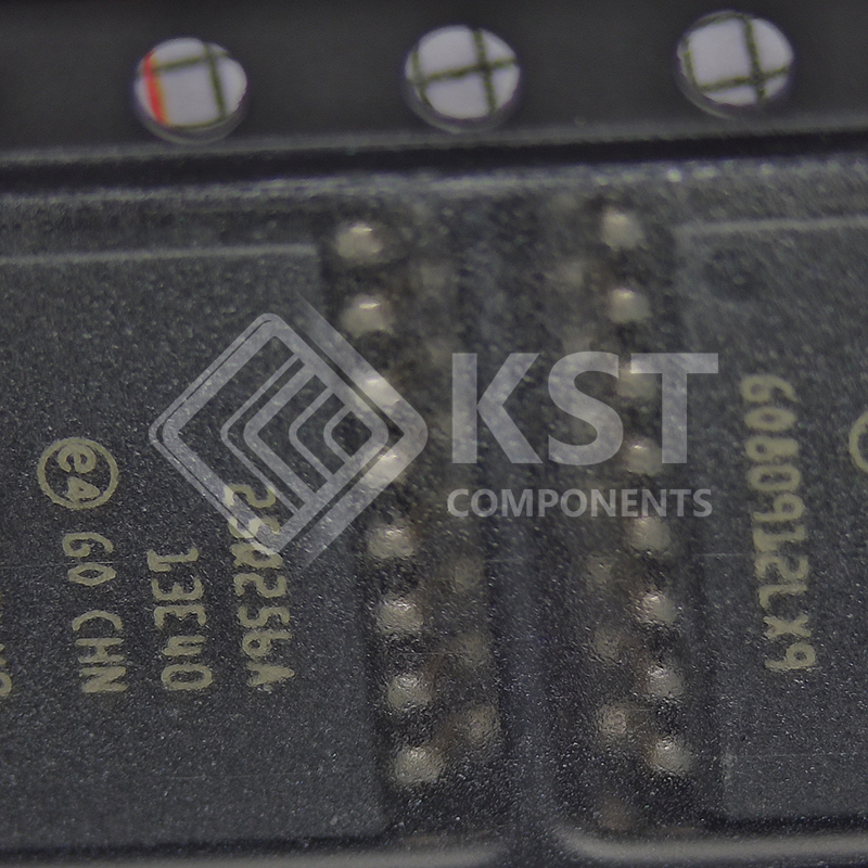
• Packages JEDEC standard, all RoHS compliant
– V-PDFN-8/8mm x 6mm (also known as SON,
DFPN, MLP, MLF)
– SOP2-16/300mils (also known as SO16W, SO16-
Wide, SOIC-16)
– T-PBGA-24b05/6mm x 8mm (also known as
TBGA24)