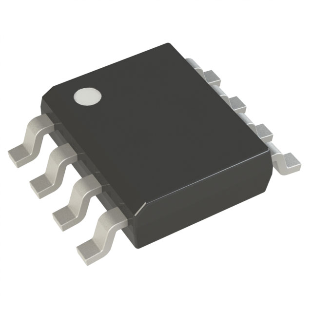
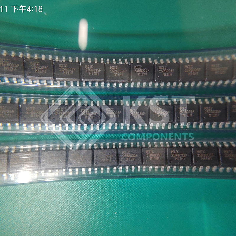
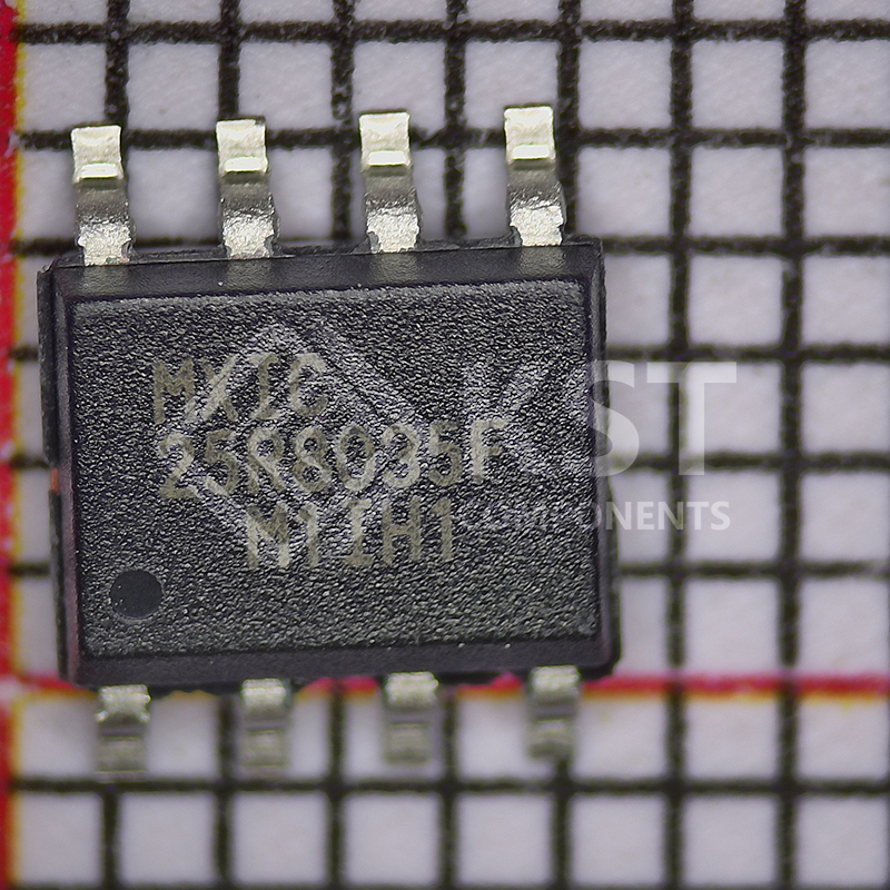
MX25R8035FM1IH1

MX25R8035F is 8Mb bits Serial NOR Flash memory, which is configured as 1,048,576 x 8 internally. When it is in
four I/O mode, the structure becomes 2,097,152 bits x 4 or 4,194,304 bits x 2.
MX25R8035F features a serial peripheral interface and software protocol allowing operation on a simple 3-wire bus
while it is in single I/O mode. The three bus signals are a clock input (SCLK), a serial data input (SI), and a serial
data output (SO). Serial access to the device is enabled by CS# input.
When it is in two I/O read mode, the SI pin and SO pin become SIO0 pin and SIO1 pin for address/dummy bits
input and data output. When it is in four I/O read mode, the SI pin, SO pin, WP# pin and RESET#/HOLD# pin
become SIO0 pin, SIO1 pin, SIO2 pin and SIO3 pin for address/dummy bits input and data output.
The MX25R8035F MXSMIO®
(Serial Multi I/O) provides sequential read operation on the whole chip.
After program/erase command is issued, auto program/erase algorithms which program/erase and verify the
specified page or sector/block locations will be executed. Program command is executed on byte basis, or page (256
bytes) basis, or word basis. Erase command is executed on 4K-byte sector, 32K-byte block, or 64K-byte block, or
whole chip basis.
To provide user with ease of interface, a status register is included to indicate the status of the chip. The status read
command can be issued to detect completion status of a program or erase operation via WIP bit.
Advanced security features enhance the protection and security functions, please see security features section for
more details.
The MX25R8035F utilizes Macronix’s proprietary memory cell, which reliably stores memory contents even after
100,000 program and erase cycles.

Category:

Download Details PDF

Notice:

In stock will ship in 2 days. Real-time inventory pls confirm with us.

INQUIRY ONLINE


    SPECIFICATION

    • Supports Serial Peripheral Interface — Mode 0 and Mode 3
    • 8,388,608 x 1 bit structure or 4,194,304 x 2 bits (two I/O mode) structure or 2,097,152 x 4 bits (four I/O mode)
    structure
    • Equal Sectors with 4K byte each, or Equal Blocks with 32K/64K byte each
    – Any Block can be erased individually
    • Single Power Supply Operation
    – Operation Voltage: 1.65V-3.6V for Read, Erase and Program Operations
    • Latch-up protected to 100mA from -1V to Vcc +1V