


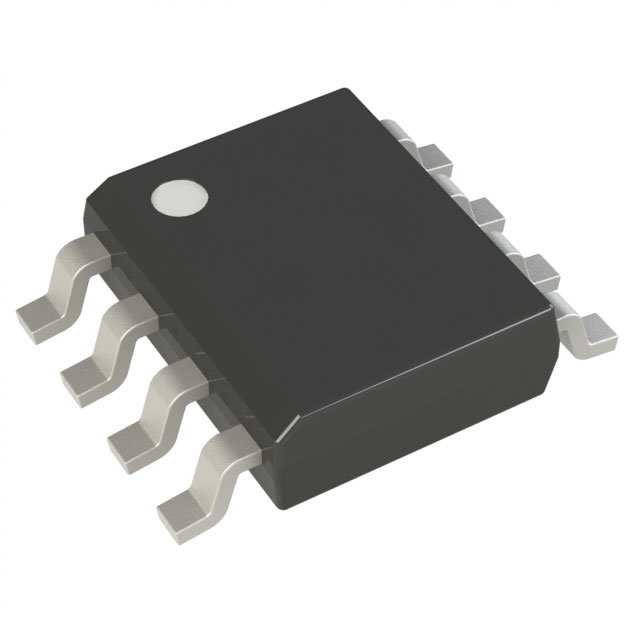
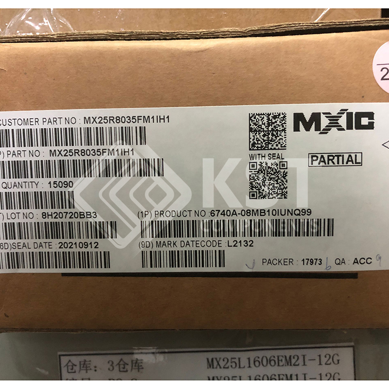
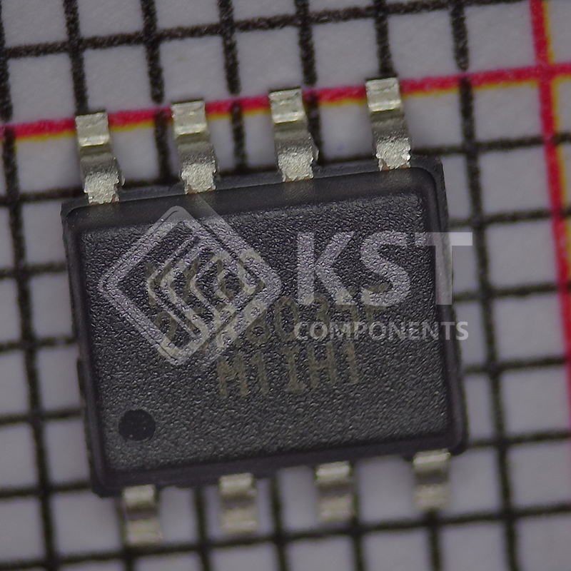
MX25R8035FM1IH1
INQUIRY ONLINE
GENERAL
• Supports Serial Peripheral Interface — Mode 0 and Mode 3
• 8,388,608 x 1 bit structure or 4,194,304 x 2 bits (two I/O mode) structure or 2,097,152 x 4 bits (four I/O mode)
structure
• Equal Sectors with 4K byte each, or Equal Blocks with 32K/64K byte each
– Any Block can be erased individually
• Single Power Supply Operation
– Operation Voltage: 1.65V-3.6V for Read, Erase and Program Operations
• Latch-up protected to 100mA from -1V to Vcc +1V
PERFORMANCE
• High Performance
– Fast read
– 1 I/O: 108MHz with 8 dummy cycles
– 2 I/O: 104MHz with 4 dummy cycles, equivalent to 208MHz
– 4 I/O: 104MHz with 2+4 dummy cycles, equivalent to 416MHz
– Fast program and erase time
– 8/16/32/64 byte Wrap-Around Burst Read Mode
• Ultra Low Power Consumption
• Minimum 100,000 erase/program cycles
• 20 years data retention
SOFTWARE FEATURES
• Input Data Format
– 1-byte Command code
• Advanced Security Features
– Block lock protection
The BP0-BP3 status bit defines the size of the area to be software protection against program and erase
instructions
• Additional 8K bits secured OTP
– Features unique identifier.
– Factory locked identifiable and customer lockable
• Auto Erase and Auto Program Algorithm
– Automatically erases and verifies data at selected sector or block
– Automatically programs and verifies data at selected page by an internal algorithm that automatically times the
program pulse widths (Any page to be programed should have page in the erased state first)
• Status Register Feature
• Command Reset
• Program/Erase Suspend and Program/Erase Resume
• Electronic Identification
– JEDEC 1-byte manufacturer ID and 2-byte device ID
– RES command for 1-byte Device ID
– REMS command for 1-byte manufacturer ID and 1-byte device ID
• Support Serial Flash Discoverable Parameters (SFDP) mode
• Support Unique ID (Please contact local Macronix sales for detail information)
HARDWARE FEATURES
• SCLK Input
– Serial clock input
• SI/SIO0
– Serial Data Input or Serial Data Input/Output for 2 x I/O read mode and 4 x I/O read mode
• SO/SIO1
– Serial Data Output or Serial Data Input/Output for 2 x I/O read mode and 4 x I/O read mode
• WP#/SIO2
– Hardware write protection or serial data Input/Output for 4 x I/O read mode
• RESET#/SIO3 * or HOLD#/SIO3 *
– Hardware Reset pin or Serial input & Output for 4 x I/O read mode
or
– HOLD feature, to pause the device without deselecting the device or Serial input & Output for 4 x I/O read mode
* Depends on part number options
• PACKAGE
– 8-pin SOP (150mil/200mil)
– 8-land WSON (6x5mm)
– 8-land USON (2x3mm)
– 8-ball WLCSP (3-2-3 Ball Array)
– 8-ball WLCSP (2×4 Ball Array)
– All devices are RoHS Compliant and Halogen-free