


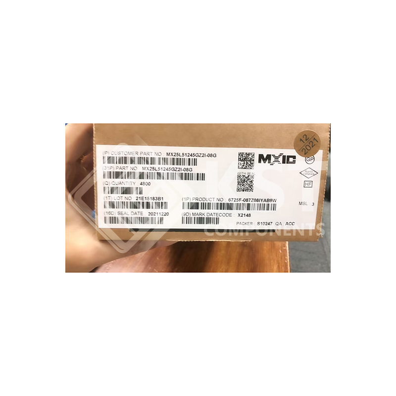
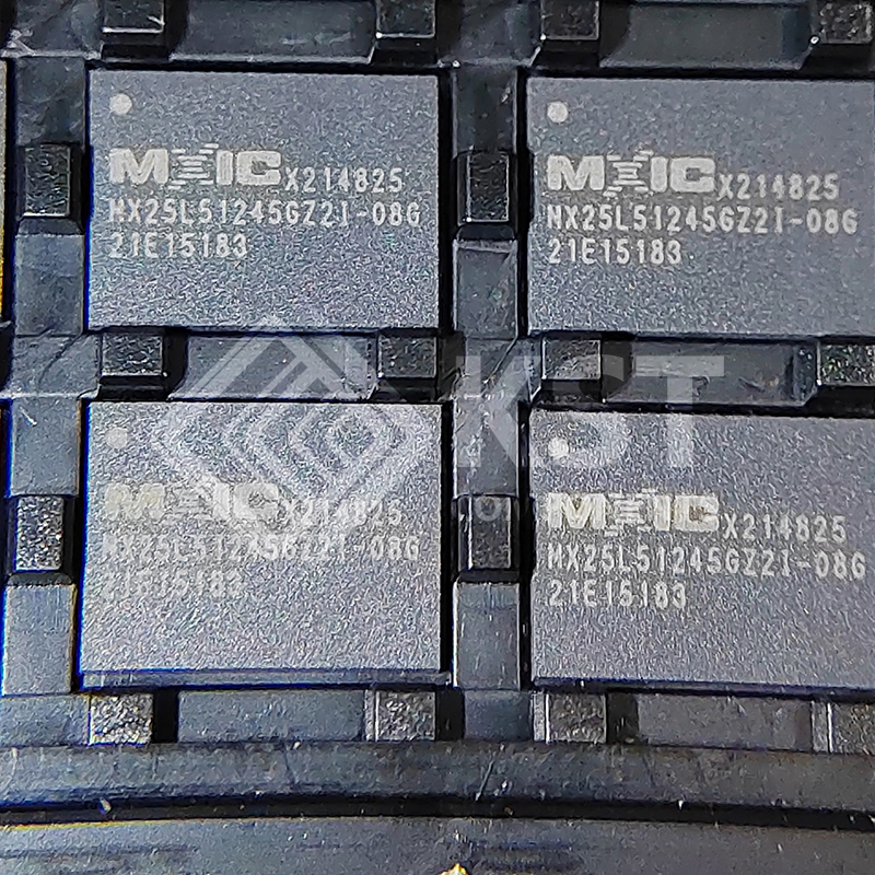
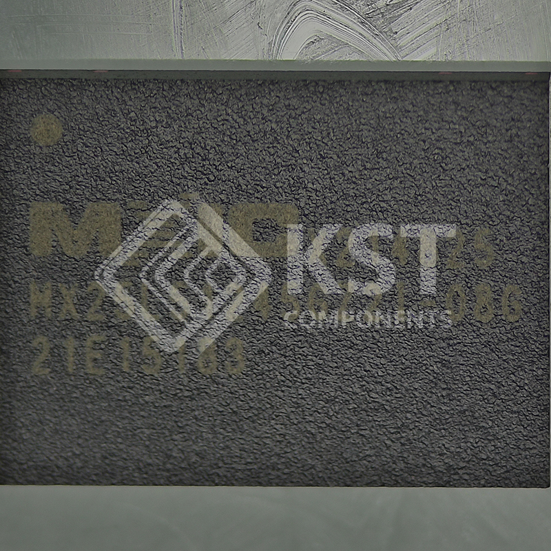
MX25L51245GZ2I-08G
INQUIRY ONLINE
GENERAL
• Supports Serial Peripheral Interface — Mode 0 and
Mode 3
• Single Power Supply Operation
– 2.7 to 3.6 volts for read, erase, and program operations
• 536,870,912 x 1 bit structure
or 268,435,456 x 2 bits (two I/O mode) structure
or 134,217,728 x 4 bits (four I/O mode) structure
• Protocol Support
– Single I/O, Dual I/O and Quad I/O
• Latch-up protected to 100mA from -1V to Vcc +1V
• Fast read for SPI mode
– Supports clock frequencies up to 166MHz for all
protocols
– Supports Fast Read, 2READ, DREAD, 4READ,
QREAD instructions
– Supports DTR (Double Transfer Rate) Mode
– Configurable dummy cycle number for fast read
operation
• Supports Performance Enhance Mode – XIP
(execute-in-place)
• Quad Peripheral Interface (QPI) available
• Equal 4K byte sectors, or Equal Blocks with 32K
bytes or 64K bytes each
– Any Block can be erased individually
• Programming :
– 256byte page buffer
– Quad Input/Output page program(4PP) to enhance
program performance
• Typical 100,000 erase/program cycles
• 20 years data retention
SOFTWARE FEATURES
• Input Data Format
– 1-byte Command code
• Advanced Security Features
– Block lock protection
The BP0-BP3 and T/B status bits define the size
of the area to be protected against program and
erase instructions
– Advanced sector protection function (Solid and
Password Protect)
• Additional 4K bit security OTP
– Features unique identifier
– Factory locked identifiable, and customer lockable
• Command Reset
• Program/Erase Suspend and Resume operation
• Electronic Identification
– JEDEC 1-byte manufacturer ID and 2-byte device ID
– RES command for 1-byte Device ID
– REMS command for 1-byte manufacturer ID and
1-byte device ID
• Supports Serial Flash Discoverable Parameters
(SFDP) mode
HARDWARE FEATURES
• SCLK Input
– Serial clock input
• SI/SIO0
– Serial Data Input or Serial Data Input/Output for
2 x I/O read mode and 4 x I/O read mode
• SO/SIO1
– Serial Data Output or Serial Data Input/Output
for 2 x I/O read mode and 4 x I/O read mode
• WP#/SIO2
– Hardware write protection or serial data Input/
Output for 4 x I/O read mode
• RESET#/SIO3
– Hardware Reset pin or Serial input & Output for
4 x I/O read mode
• NC/SIO3
– No connection or Serial Data Input/Output for 4 x
I/O read mode
• RESET#
– Hardware Reset pin
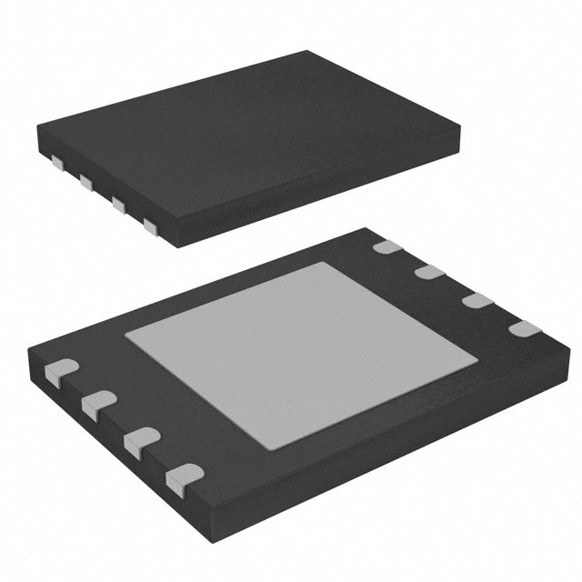
• PACKAGE
– 16-pin SOP (300mil)
– 8-land WSON (8x6mm)
– 24-Ball BGA (5×5 ball array)
– All devices are RoHS Compliant and Halogen-free