


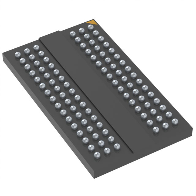
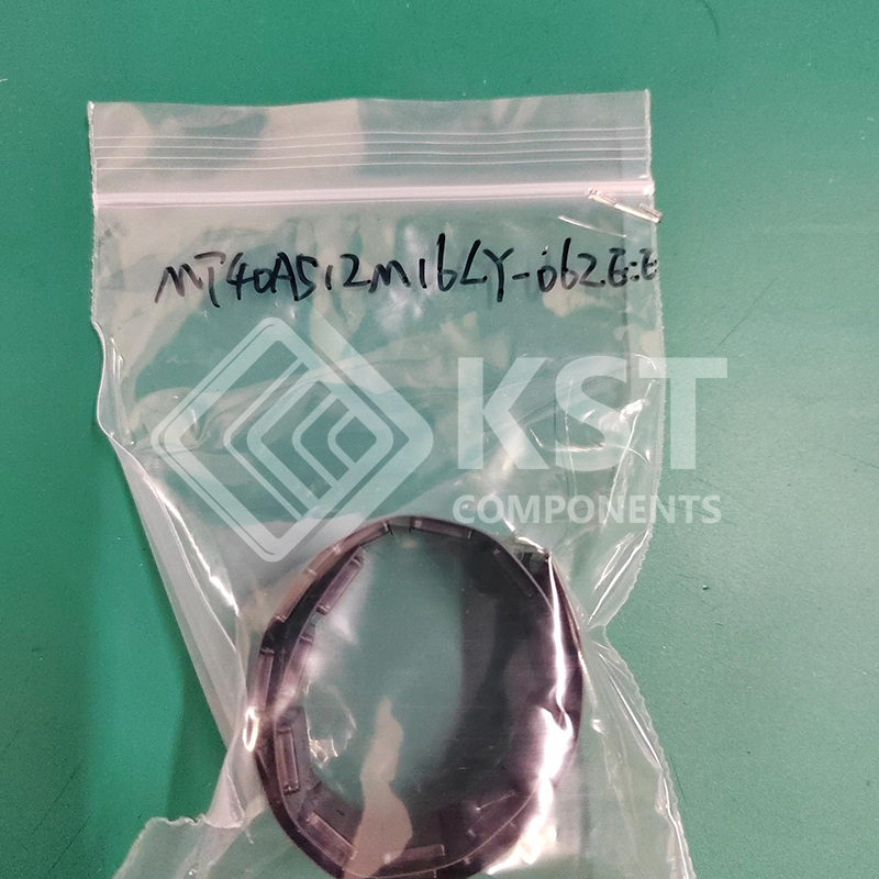
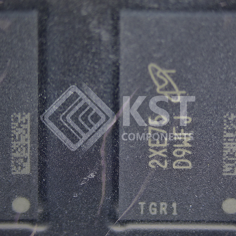
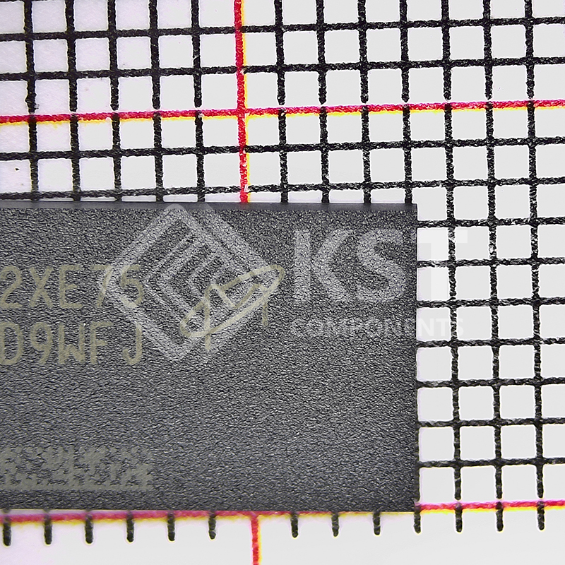
MT40A512M16LY-062E:E
INQUIRY ONLINE
• VDD = VDDQ = 1.2V ±60mV
• VPP = 2.5V –125mV/+250mV
• On-die, internal, adjustable VREFDQ generation
• 1.2V pseudo open-drain I/O
• Refresh time of 8192-cycle at TC temperature range:
– 64ms at –40°C to 85°C
– 32ms at 85°C to 95°C
– 16ms at 95°C to 105°C
– 8ms at 105°C to 125°C
• 16 internal banks (x8): 4 groups of 4 banks each
• 8 internal banks (x16): 2 groups of 4 banks each
• 8n-bit prefetch architecture
• Programmable data strobe preambles
• Data strobe preamble training
• Command/Address latency (CAL)
• Multipurpose register read and write capability
• Write leveling
• Self refresh mode
• Low-power auto self refresh (LPASR)
• Temperature controlled refresh (TCR)
• Fine granularity refresh
• Self refresh abort
• Maximum power saving
• Output driver calibration
• Nominal, park, and dynamic on-die termination
(ODT)
• Data bus inversion (DBI) for data bus
• Command/Address (CA) parity
• Databus write cyclic redundancy check (CRC)
• Per-DRAM addressability
• Connectivity test
• JEDEC JESD-79-4 compliant
• sPPR and hPPR capability
• AEC-Q100
• PPAP submission
Options1 Marking
• Configuration
– 1 Gig x 8 1G8
– 512 Meg x 16 512M16
• 78-ball FBGA package (Pb-free) – x8
– 8mm x 12mm – Rev. B WE
– 7.5mm x 11mm – Rev. E SA
• 96-ball FBGA package (Pb-free) – x16
– 8mm x 14mm – Rev. B JY
– 7.5mm x 13.5mm – Rev. E LY
• Timing – cycle time
– 0.625ns @ CL = 22 (DDR4-3200) -062E
– 0.750ns @ CL = 18 (DDR4-2666) -075E
– 0.833ns @ CL = 16 (DDR4-2400) -083E
• Product certification
– Automotive A
• Operating temperature
– Industrial (–40° ≤ TC ≤ 95°C) IT
– Automotive (–40° ≤ TC ≤ 105°C) AT
– Ultra-high (–40° ≤ TC ≤ 125°C)3 UT
• Revision :B, :E
Notes: 1. Not all options listed can be combined to
define an offered product. Use the part
catalog search on http://www.micron.com
for available offerings.
2. The ×4 device is not offered and the mode
is not supported by the x8 or x16 device
even though some ×4 mode descriptions exist in the datasheet.
3. The UT option use based on automotive usage model. Contact Micron sales representative if you have questions.
4. -062E is only available for die Rev. E.