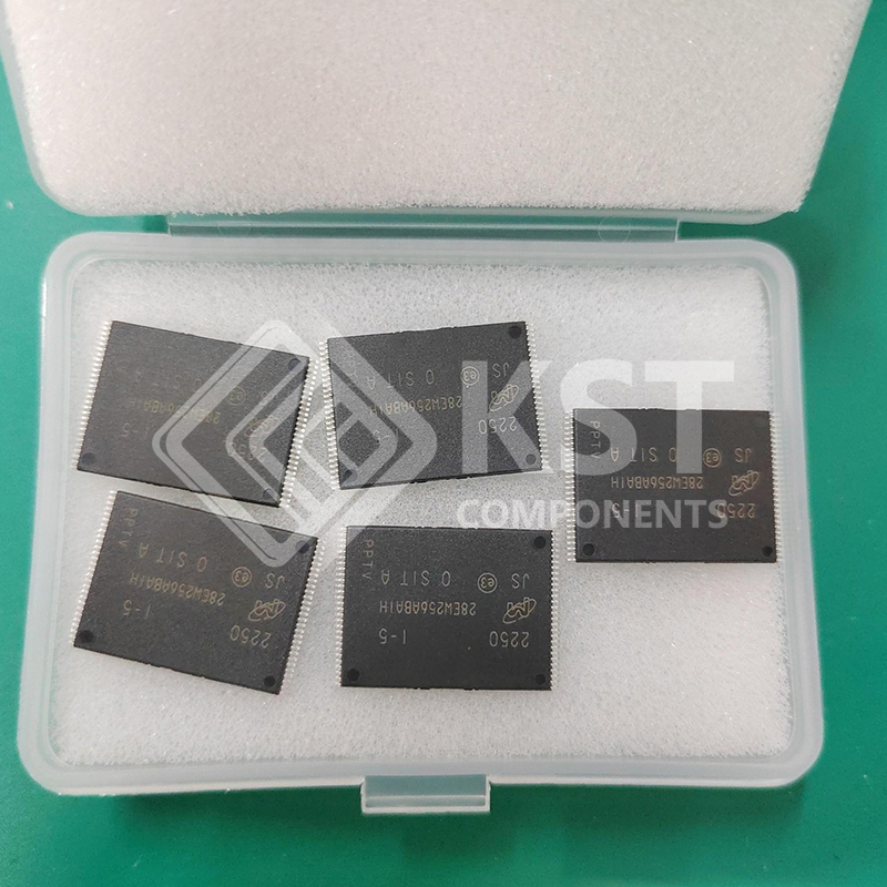
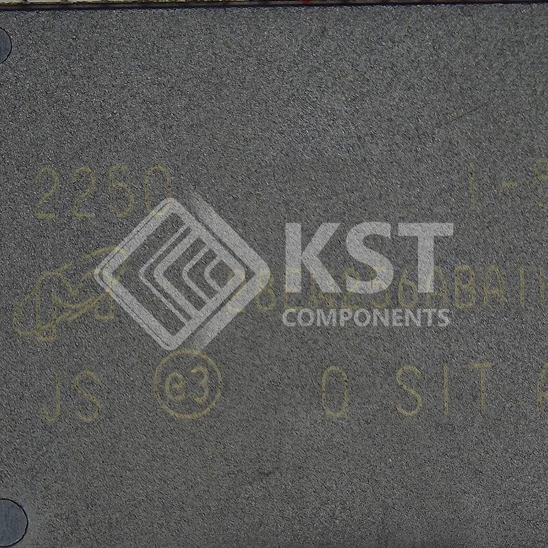
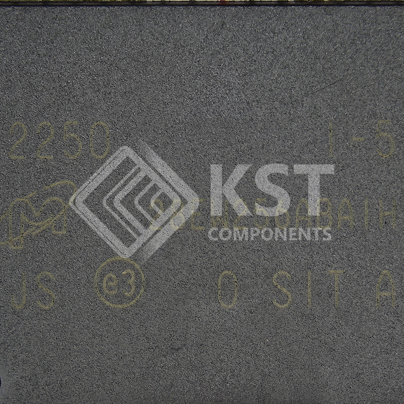
MT28EW256ABA1HJS-0SIT

The device is an asynchronous, uniform block, parallel NOR Flash memory device.
READ, ERASE, and PROGRAM operations are performed using a single low-voltage supply. Upon power-up, the device defaults to read array mode.
The main memory array is divided into uniform blocks that can be erased independently so that valid data can be preserved while old data is purged. PROGRAM and ERASE
commands are written to the command interface of the memory. An on-chip program/
erase controller simplifies the process of programming or erasing the memory by taking
care of all special operations required to update the memory contents. The end of a
PROGRAM or ERASE operation can be detected and any error condition can be identified. The command set required to control the device is consistent with JEDEC standards.
CE#, OE#, and WE# control the bus operation of the device and enable a simple connection to most microprocessors, often without additional logic.
The device supports asynchronous random read and page read from all blocks of the
array. It also features an internal program buffer that improves throughput by programming 512 words via one command sequence. A 128-word extended memory block overlaps addresses with array block 0. Users can program this additional space and then
protect it to permanently secure the contents. The device also features different levels of
hardware and software protection to secure blocks from unwanted modification.

Category:

Download Details PDF

Notice:

In stock will ship in 2 days. Real-time inventory pls confirm with us.

INQUIRY ONLINE


    SPECIFICATION

    • Single-level cell (SLC) process technology
    • Density: 256Mb
    • Supply voltage
    – VCC = 2.7–3.6V (program, erase, read)
    – VCCQ = 1.65 – VCC (I/O buffers)
    • Asynchronous random/page read
    – Page size: 16 words or 32 bytes
    – Page access: 20ns
    – Random access: 70ns (VCC = VCCQ = 2.7-3.6V)
    – Random access: 75ns (VCCQ = 1.65-VCC)
    • Buffer program (512-word program buffer)
    – 2.0 MB/s (TYP) when using full buffer program
    – 2.5 MB/s (TYP) when using accelerated buffer
    program (VHH)
    • Word/Byte program: 25us per word (TYP)
    • Block erase (128KB): 0.2s (TYP)
    • Memory organization
    – Uniform blocks: 128KB or 64KW each
    – x8/x16 data bus
    • Program/erase suspend and resume capability
    – Read from another block during a PROGRAM
    SUSPEND operation
    – Read or program another block during an ERASE
    SUSPEND operation
    • Unlock bypass, block erase, chip erase, and write to
    buffer capability
    • BLANK CHECK operation to verify an erased block
    • CYCLIC REDUNDANCY CHECK (CRC) operation to
    verify a program pattern
    • VPP/WP# protection
    – Protects first or last block regardless of block
    protection settings
    • Software protection
    – Volatile protection
    – Nonvolatile protection
    – Password protection
    • Extended memory block
    – 128-word (256-byte) block for permanent, secure
    identification
    – Programmed or locked at the factory or by the
    customer
    • JESD47-compliant
    – 100,000 (minimum) ERASE cycles per block
    – Data retention: 20 years (TYP)
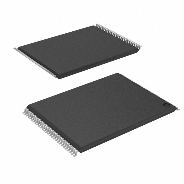
    • Package
    – 56-pin TSOP, 14 x 20mm (JS)
    – 64-ball LBGA, 11 x 13mm (PC)
    – 56-ball VFBGA, 7 x 9mm (PN)
    • RoHS-compliant, halogen-free packaging
    • Operating temperature
    – Ambient: –40°C to +85°C