


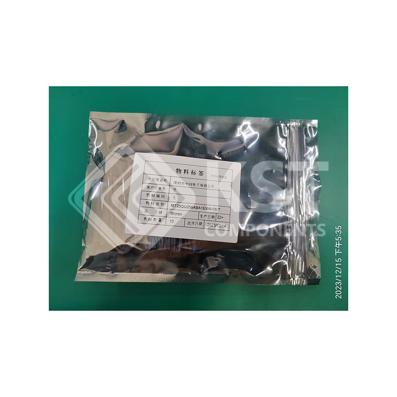
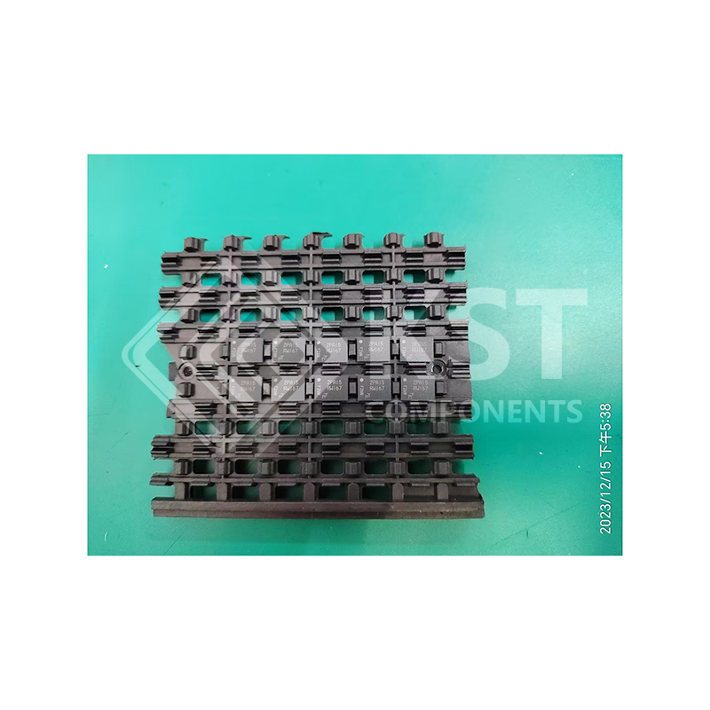
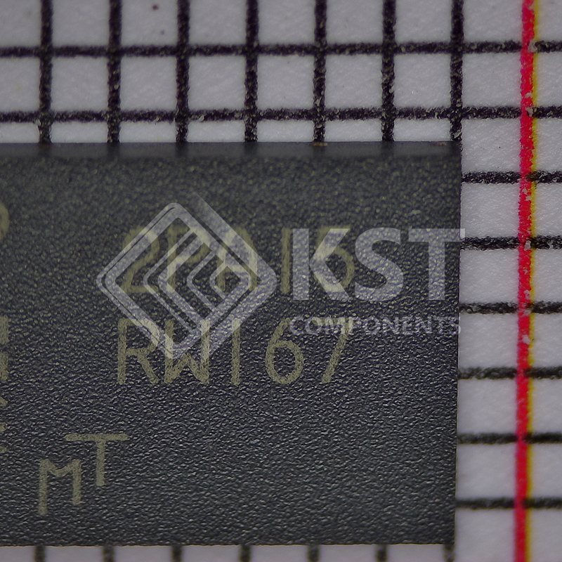
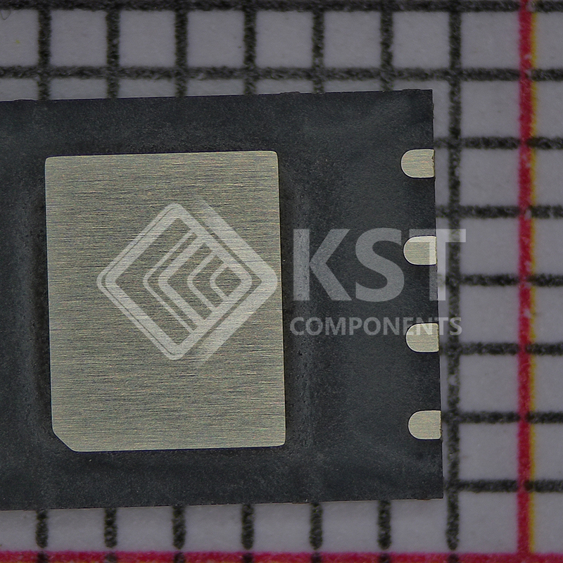
MT25QU256ABA1EW9-0SIT
INQUIRY ONLINE
• SPI-compatible serial bus interface
• Single and double transfer rate (STR/DTR)
• Clock frequency
– 166 MHz (MAX) for all protocols in STR
– 90 MHz (MAX) for all protocols in DTR
• Dual/quad I/O commands for increased
throughput up to 90 MB/s
• Supported protocols in both STR and DTR
– Extended I/O protocol
– Dual I/O protocol
– Quad I/O protocol
• Execute-in-place (XIP)
• PROGRAM/ERASE SUSPEND operations
• Volatile and nonvolatile configuration settings
• Software reset
• Additional reset pin for selected part numbers
• 3-byte and 4-byte address modes: enable memory
access beyond 128Mb
• Dedicated 64-byte OTP area outside main memory
– Readable and user-lockable
– Permanent lock with PROGRAM OTP command
• Erase capability
– Bulk erase
– Sector erase 64KB uniform granularity
– Subsector erase 4KB, 32KB granularity
• Erase performance: 400KB/sec (64KB sector)
• Erase performance: 80KB/sec (4KB sub-sector)
• Program performance: 2MB/sec
• Security and write protection
– Volatile and nonvolatile locking and software
write protection for each 64KB sector
– Nonvolatile configuration locking
– Password protection
– Hardware write protection: nonvolatile bits
(BP[3:0] and TB) define protected area size
– Program/erase protection during power-up
– CRC detects accidental changes to raw data
• Electronic signature
-JEDEC-standard 3-byte signature (BB19h)
– Extended device ID: two additional bytes identify
device factory options
• JESD47H-compliant
– Minimum 100,000 ERASE cycles per sector
– Data retention: 20 years (TYP)
• Voltage
– 1.7–2.0V U
• Density
– 256Mb 256
• Device stacking
– Monolithic A
• Device generation B
• Die revision A
• Pin configuration
– RESET# and HOLD# 8
• Sector Size
– 64KB E
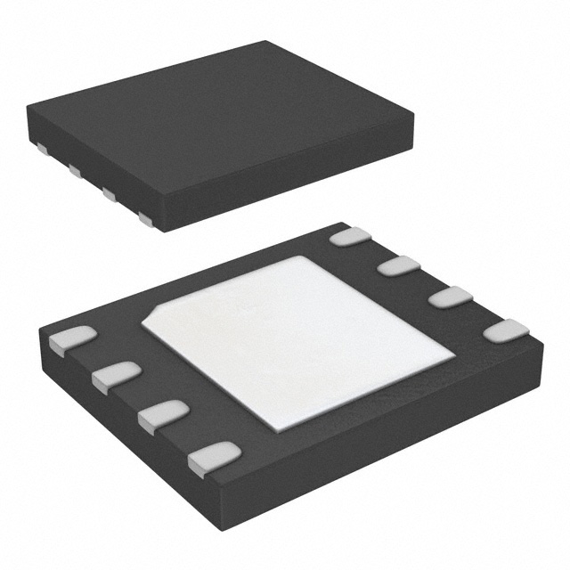
• Packages – JEDEC-standard, RoHScompliant
– 24-ball T-PBGA 05/6mm x 8mm
(5 x 5 array)
12
– Wafer level chip-scale package,
23 balls, 9 active balls (XFWLBGA
0.5P)
55
– 16-pin SOP2, 300 mils
(S016W, S016-Wide, SOIC-16)
SF
– W-PDFN-8 6mm x 5mm
(MLP8 6mm x 5mm)
W7
– W-PDFN-8 8mm x 6mm
(MLP8 8mm x 6mm)
W9
• Security features
– Standard security 0
– Advanced security 1
– RPMC enabled M
• Special options
– Standard S
– Automotive A
• Operating temperature range
– From –40°C to +85°C IT
– From –40°C to +105°C AT
– From –40°C to +125°C UT