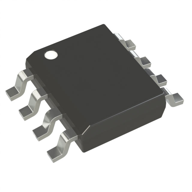
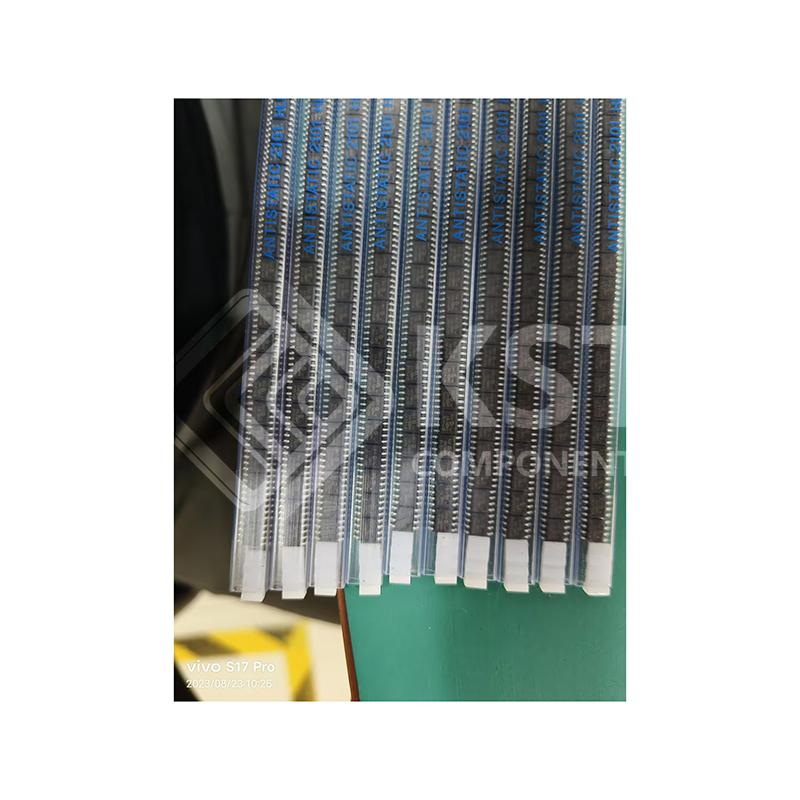
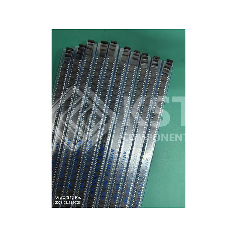
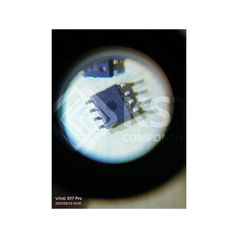
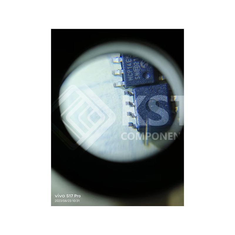
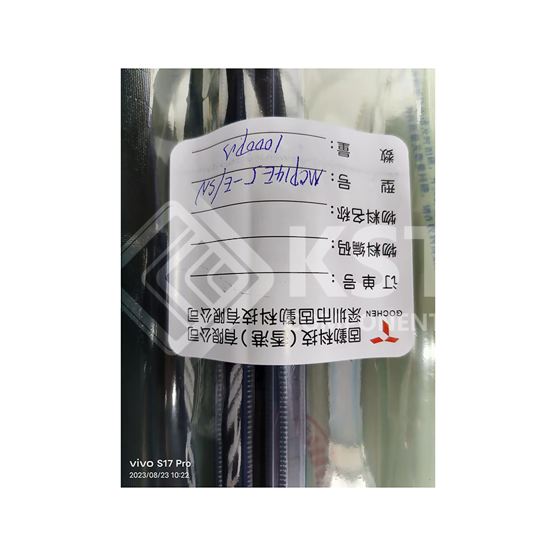
MCP14E5-E/SN

The MCP14E3/MCP14E4/MCP14E5 devices are a
family of 4.0A buffers/MOSFET drivers. Dual-inverting,
dual-noninvertering, and complementary outputs are
standard logic options offered.
The MCP14E3/MCP14E4/MCP14E5 drivers are
capable of operating from a 4.5V to 18V single power
supply and can easily charge and discharge 2200 pF
gate capacitance in under 15 ns (typical). They provide
low impedance in both the ON and OFF states to
ensure the MOSFET’s intended state will not be
affected, even by large transients. The MCP14E3/
MCP14E4/MCP14E5 inputs may be driven directly
from either TTL or CMOS (2.4V to 18V).
Additional control of the MCP14E3/MCP14E4/
MCP14E5 outputs is allowed by the use of separate
enable functions. The ENB_A and ENB_B pins are
active high and are internally pulled up to VDD. The pins
maybe left floating for standard operation.
The MCP14E3/MCP14E4/MCP14E5 dual-output 4.0A
driver family is offered in both surface-mount and pinthrough-hole packages with a -40°C to +125°C
temperature rating. The low thermal resistance of the
thermally enhanced DFN package allows for greater
power dissipation capability for driving heavier
capacitive or resistive loads.
These devices are highly latch-up resistant under any
conditions within their power and voltage ratings. They
are not subject to damage when up to 5V of noise
spiking (of either polarity) occurs on the ground pin.
They can accept, without damage or logic upset, up to
1.5A of reverse current being forced back into their
outputs. All terminals are fully protect against
Electrostatic Discharge (ESD) up to 4 kV.


Download Details PDF

Notice:

In stock will ship in 2 days. Real-time inventory pls confirm with us.

INQUIRY ONLINE


    SPECIFICATION

    • High Peak Output Current: 4.0A (typical)
    • Independent Enable Function for Each Driver
    Output
    • Low Shoot-Through/Cross-Conduction Current in
    Output Stage
    • Wide Input Supply Voltage Operating Range:
    – 4.5V to 18V
    • High Capacitive Load Drive Capability:
    – 2200 pF in 15 ns (typical)
    – 5600 pF in 26 ns (typical)
    • Short Delay Times: 50 ns (typical)
    • Latch-Up Protected: Will Withstand 1.5A Reverse
    Current
    • Logic Input Will Withstand Negative Swing Up To
    5V
    • Space-Saving Packages:
    – 8-Lead 6×5 DFN, PDIP, SOIC