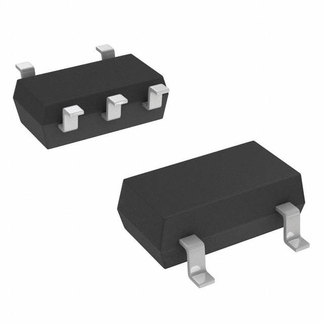
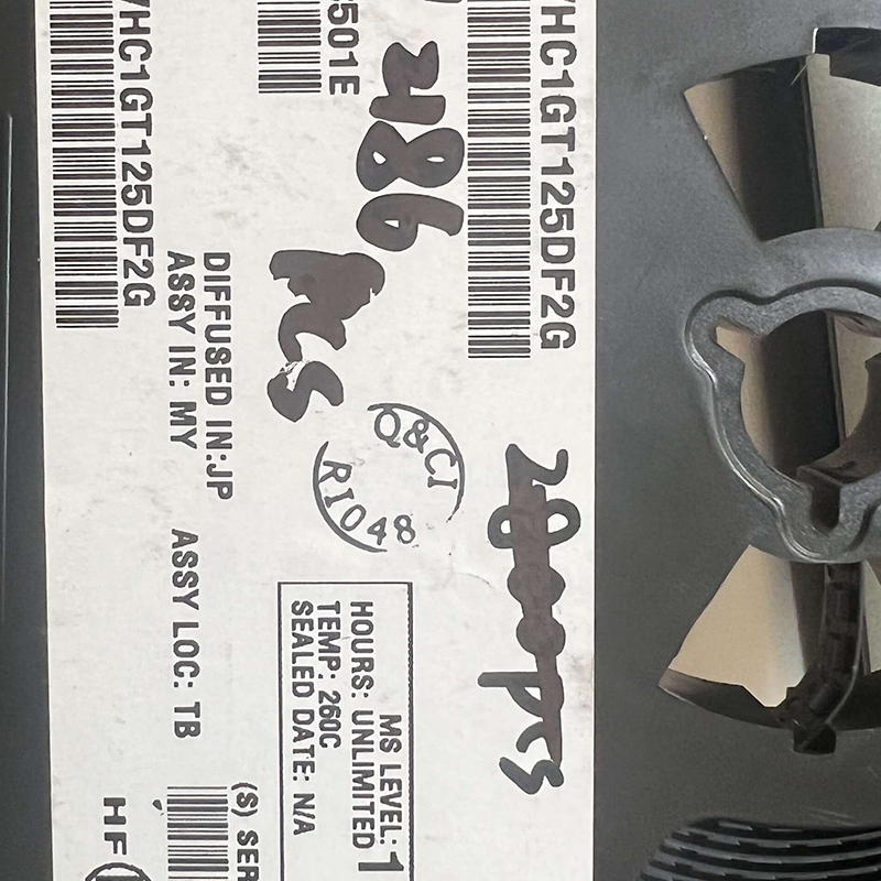
M74VHC1GT125DF2G

The MC74VHC1G125 / MC74VHC1GT125 is a single
non−inverting 3−state buffer in tiny footprint packages. The
MC74VHC1G125 has CMOS−level input thresholds while the
MC74VHC1GT125 has TTL−level input thresholds.
The internal circuit is composed of three stages, including a buffered
3−state output which provides high noise immunity and stable output.
The input structures provide protection when voltages up to 5.5 V
are applied, regardless of the supply voltage. This allows the device to
be used to interface 5 V circuits to 3 V circuits. Some output structures
also provide protection when VCC = 0 V and when the output voltage
exceeds VCC. These input and output structures help prevent device
destruction caused by supply voltage − input/output voltage mismatch,
battery backup, hot insertion, etc.

Category:

Download Details PDF

Notice:

In stock will ship in 2 days. Real-time inventory pls confirm with us.

INQUIRY ONLINE


    SPECIFICATION

    • Designed for 2.0 V to 5.5 V VCC Operation
    • 3.5 ns tPD at 5 V (typ)
    • Inputs/Outputs Over−Voltage Tolerant up to 5.5 V
    • IOFF Supports Partial Power Down Protection
    • Source/Sink 8 mA at 3.0 V
    • Available in SC−88A, SC−74A, SOT−953 and UDFN6 Packages
    • Chip Complexity < 100 FETs
    • −Q Suffix for Automotive and Other Applications Requiring Unique
    Site and Control Change Requirements; AEC−Q100 Qualified and
    PPAP Capable
    • These Devices are Pb−Free, Halogen Free/BFR Free and are RoHS
    Compliant