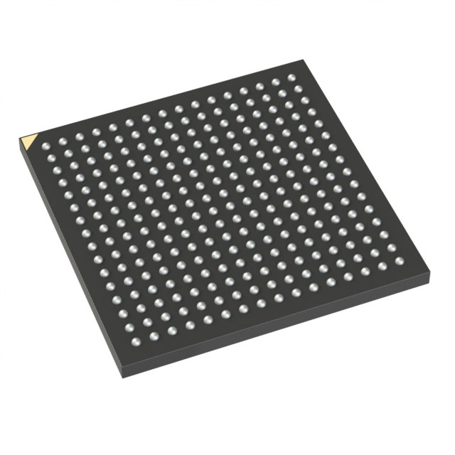
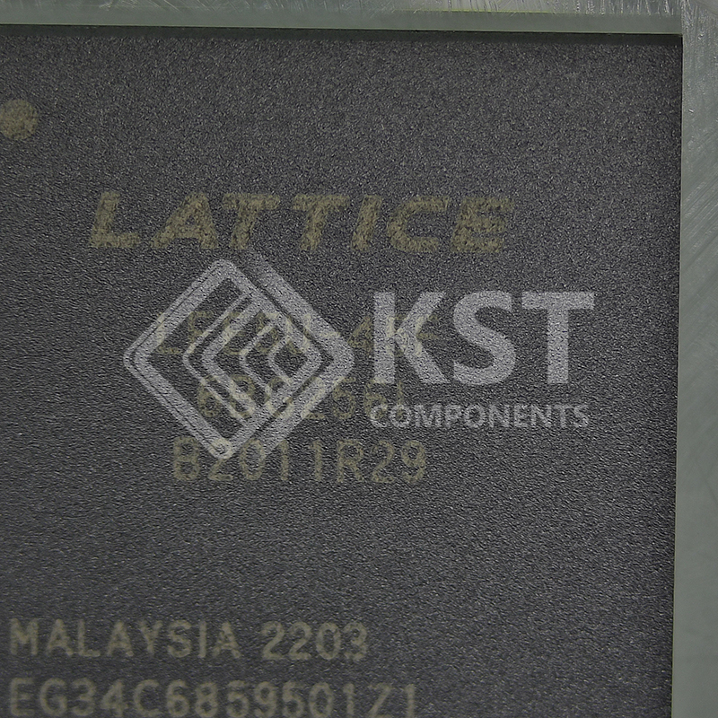
LFE5U-45F-6BG256I

Each ECP5/ECP5-5G device contains an array of logic blocks surrounded by Programmable I/O Cells (PIC). Interspersed
between the rows of logic blocks are rows of sysMEM™ Embedded Block RAM (EBR) and rows of sysDSP™ Digital Signal
Processing slices, as shown in Figure 2.1. The LFE5-85 devices have three rows of DSP slices, the LFE5-45 devices have
two rows, and both LFE5-25 and LFE5-12 devices have one. In addition, the LFE5UM/LFE5UM5G devices contain
SERDES Duals on the bottom of the device.
The Programmable Functional Unit (PFU) contains the building blocks for logic, arithmetic, RAM, and ROM functions.
The PFU block is optimized for flexibility, allowing complex designs to be implemented quickly and efficiently. Logic
Blocks are arranged in a two-dimensional array.
The ECP5/ECP5-5G devices contain one or more rows of sysMEM EBR blocks. sysMEM EBRs are large, dedicated 18 Kb
fast memory blocks. Each sysMEM block can be configured in a variety of depths and widths as RAM or ROM. In
addition, ECP5/ECP5-5G devices contain up to three rows of DSP slices. Each DSP slice has multipliers and
adder/accumulators, which are the building blocks for complex signal processing capabilities.
The ECP5 devices feature up to four embedded 3.2 Gb/s SERDES channels, and the ECP5-5G devices feature up to four
embedded 5 Gb/s SERDES channels. Each SERDES channel contains independent 8b/10b encoding / decoding, polarity
adjust and elastic buffer logic. Each group of two SERDES channels, along with its Physical Coding Sublayer (PCS) block,
creates a dual DCU (Dual Channel Unit). The functionality of the SERDES/PCS duals can be controlled by SRAM cell
settings during device configuration or by registers that are addressable during device operation. The registers in every
dual can be programmed via the SERDES Client Interface (SCI). These DCUs (up to two) are located at the bottom of the
devices.
Each PIC block encompasses two PIOs (PIO pairs) with their respective sysI/O buffers. The sysI/O buffers of the
ECP5/ECP5-5G devices are arranged in seven banks (eight banks for LFE5-85 devices in caBGA756 and caBGA554
packages), allowing the implementation of a wide variety of I/O standards. One of these banks (Bank 8) is shared with
the programming interfaces. Half of the PIO pairs on the left and right edges of the device can be configured as LVDS
transmit pairs, and all pairs on left and right can be configured as LVDS receive pairs. The PIC logic in the left and right
banks also includes pre-engineered support to aid in the implementation of high speed source synchronous standards
such as XGMII, 7:1 LVDS, along with memory interfaces including DDR3 and LPDDR3.
The ECP5/ECP5-5G registers in PFU and sysI/O can be configured to be SET or RESET. After power up and the device is
configured, it enters into user mode with these registers SET/RESET according to the configuration setting, allowing the
device entering to a known state for predictable system function.
Other blocks provided include PLLs, DLLs and configuration functions. The ECP5/ECP5-5G architecture provides up to
four Delay-Locked Loops (DLLs) and up to four Phase-Locked Loops (PLLs). The PLL and DLL blocks are located at the
corners of each device.
The configuration block that supports features such as configuration bit-stream decryption, transparent updates and
dual-boot support is located at the bottom of each device, to the left of the SERDES blocks. Every device in the
ECP5/ECP5-5G family supports a sysCONFIG™ ports located in that same corner, powered by VCCIO8, allowing for serial
or parallel device configuration.
In addition, every device in the family has a JTAG port. This family also provides an on-chip oscillator and soft error
detect capability. The ECP5 devices use 1.1 V and ECP5UM5G devices use 1.2 V as their core voltage.


Download Details PDF

Notice:

In stock will ship in 2 days. Real-time inventory pls confirm with us.

INQUIRY ONLINE


    SPECIFICATION

     Higher Logic Density for Increased System
    Integration
     12K to 84K LUTs
     197 to 365 user programmable I/O
     Embedded SERDES
     270 Mb/s, up to 3.2 Gb/s, SERDES interface
    (ECP5)
     270 Mb/s, up to 5.0 Gb/s, SERDES interface
    (ECP5-5G)
     Supports eDP in RDR (1.62 Gb/s) and HDR
     (2.7 Gb/s)
     Up to four channels per device: PCI Express,
    Ethernet (1GbE, SGMII, XAUI), and CPRI
     sysDSP™
     Fully cascadable slice architecture
     12 to 160 slices for high performance multiply
    and accumulate
     Powerful 54-bit ALU operations
     Time Division Multiplexing MAC Sharing
     Rounding and truncation
     Each slice supports
     Half 36 x 36, two 18 x 18 or four
    9 x 9 multipliers
     Advanced 18 x 36 MAC and
    18 x 18 Multiply-Multiply-Accumulate
    (MMAC) operations
     Flexible Memory Resources
     Up to 3.744 Mb sysMEM™ Embedded Block
     RAM (EBR)
     194K to 669K bits distributed RAM

     sysCLOCK Analog PLLs and DLLs
     Four DLLs and four PLLs in LFE5-45 and
    LFE5-85; two DLLs and two PLLs in LFE5-25
    and LFE5-12
     Pre-Engineered Source Synchronous I/O
     DDR registers in I/O cells
     Dedicated read/write levelling functionality
     Dedicated gearing logic
     Source synchronous standards support
     ADC/DAC, 7:1 LVDS, XGMII
     High Speed ADC/DAC devices
     Dedicated DDR2/DDR3 and LPDDR2/LPDDR3
    memory support with DQS logic, up to
    800 Mb/s data-rate
     Programmable sysI/O™ Buffer Supports Wide
    Range of Interfaces
     On-chip termination
     LVTTL and LVCMOS 33/25/18/15/12
     SSTL 18/15 I, II
     HSUL12
     LVDS, Bus-LVDS, LVPECL, RSDS, MLVDS
     subLVDS and SLVS, SoftIP MIPI D-PHY
    receiver/transmitter interfaces
     Flexible Device Configuration
     Shared bank for configuration I/O
     SPI boot flash interface
     Dual-boot images supported
     Slave SPI
     TransFR™ I/O for simple field updates
     Single Event Upset (SEU) Mitigation Support
     Soft Error Detect – Embedded hard macro
     Soft Error Correction – Without stopping user
    operation
     Soft Error Injection – Emulate SEU event to
    debug system error handling
     System Level Support
     IEEE 1149.1 and IEEE 1532 compliant
     Reveal Logic Analyzer
     On-chip oscillator for initialization and general
    use
     V core power supply for ECP5, 1.2 V core
    power supply for ECP5UM5G