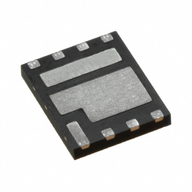
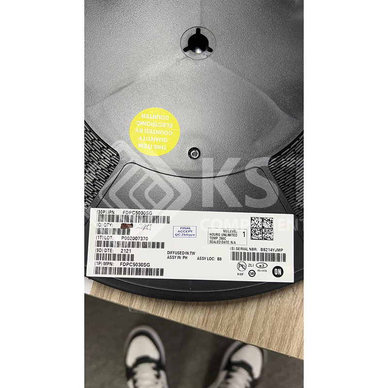
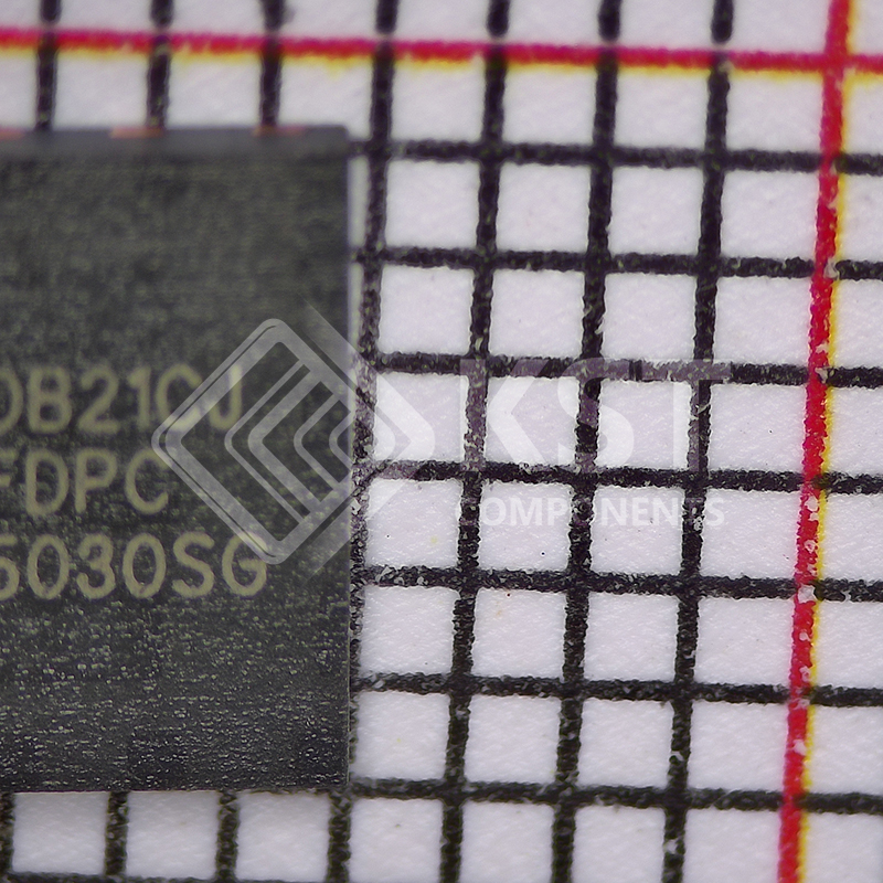
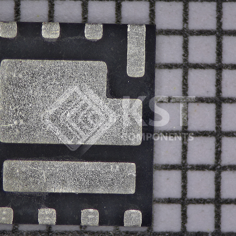
FDPC5030SG

This device includes two specialized N-Channel MOSFETs in
a dual package. The switch node has been internally connected to
enable easy placement and routing of synchronous buck converters.
The control MOSFET (Q1) and synchronous SyncFET (Q2) have
been designed to provide optimal power efficiency.

Category:

Download Details PDF

Notice:

In stock will ship in 2 days. Real-time inventory pls confirm with us.

INQUIRY ONLINE


    SPECIFICATION

    Q1: N-Channel
     Max RDS(on) = 5.0 m at VGS = 10 V, ID = 17 A
     Max RDS(on) = 6.5 m at VGS = 4.5 V, ID = 14 A
    Q2: N-Channel
     Max RDS(on) = 2.4 m at VGS = 10 V, ID = 25 A
     Max RDS(on) = 3.0 m at VGS = 4.5 V, ID = 22 A
     Low Inductance Packaging Shortens Rise/Fall Times, Resulting in
    Lower Switching Losses.
     MOSFET Integration Enables Optimum Layout for Lower Circuit
    Inductance and Reduced Switch Node Ringing.
     RoHS Compliant