CPU configuration
1K13 bits on-chip ROM
488 bits on-chip registers (SRAM,
General purpose)
5-level stacks for subroutine nesting
4 programmable level voltage detector
LVD : 4.5, 4.0, 3.3, 2.2V
3 programmable level voltage reset
LVR : 4.0, 3.5, 2.7V
Less than 1.5mA at 5V/4 MHz
Typically 15 µA, at 3V/32kHz
Typically 1 µA, during Sleep mode
I/O port configuration
2 bidirectional I/O ports : P5, P6
12 I/O pins
Wake-up port : P6
7 Programmable pull-down I/O pins
7 programmable pull-high I/O pins
7 programmable open-drain I/O pins
External interrupt with wake-up: P60
Operating voltage range:
2.1V~5.5V at 0~70C (Commercial)
2.3V~5.5V at -40~85C (Industrial)
Operating frequency range
(base on 2 clocks):
Crystal mode:
DC~20MHz/2clks @ 5V
DC~8MHz/2clks @ 3V
DC~4MHz/2clks @ 2.1V
ERC mode:
DC~2 MHz/2clks @ 2.1V
IRC mode:
Internal RC
Frequency
Drift Rate
Temperature
(-40°C~85°C)
Voltage Process Total
4 MHz ± 1%
± 3%
*(2.1~5.5V) ± 2% ± 6%
16 MHz ± 1%
± 1%
*(4.0~5.5V) ± 2% ± 4%
8 MHz ± 1%
± 2%
*(3.0~5.5V) ± 2% ± 5%
1 MHz ± 1%
± 3%
*(2.1~5.5V) ± 2% ± 6%
* Operating Voltage Range
Peripheral configuration
8-bit real time clock/counter (TCC) with selective
signal sources, trigger edges, and overflow
interrupt
External interrupt input pin
2/4 clocks per instruction cycle selected by
code option
Power down (Sleep) mode
High EFT immunity
Four available interrupts:
TCC overflow interrupt
Input-port status changed interrupt
External interrupt
Low voltage detect interrupt
Special features
Programmable free running watchdog timer
Power-on voltage detector available (1.8~1.9V)
Package type:
14-pin DIP 300mil : EM78P173ND14
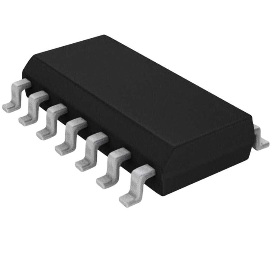
14-pin SOP 150mil : EM78P173NSO14
10-pin MSOP 118mil : EM78P173NMS10


