• Universal serial bus (USB) integration
– USB 3.2, Gen 1 and USB 2.0 peripherals compliant with USB 3.2 Specification Revision 1.0 (TID # 340800007)
– 5-Gbps SuperSpeed PHY compliant with USB 3.2 Gen 1
– High-speed On-The-Go (HS-OTG) host and peripheral compliant with OTG Supplement Version 2.0
– Thirty-two physical endpoints
• General programmable interface (GPIF™ II)
– Programmable 100-MHz GPIF II enables connectivity to a wide range of external devices
– 8-, 16-, 24-, and 32-bit data bus
– Up to 16 configurable control signals
• Fully accessible 32-bit CPU
– ARM926EJ core with 200-MHz operation
– 512-KB or 256-KB embedded SRAM
• Additional connectivity to the following peripherals
– SPI master at up to 33 MHz
– UART support of up to 4 Mbps
– I2
C master controller at 1 MHz
– I2S master (transmitter only) at sampling frequencies of 8 kHz, 16 kHz, 32 kHz, 44.1 kHz, 48 kHz, 96 kHz and
192 kHz
• Selectable clock input frequencies
– 19.2, 26, 38.4, and 52 MHz
– 19.2-MHz crystal input support
• Ultra low-power in core power-down mode
– Less than 60 µA with VBATT on and 20 µA with VBATT off
• Independent power domains for core and I/O
– Core operation at 1.2 V
– I2S, UART, and SPI operation at 1.8 to 3.3 V
– I2
C operation at 1.2 V to 3.3 V
• Package options
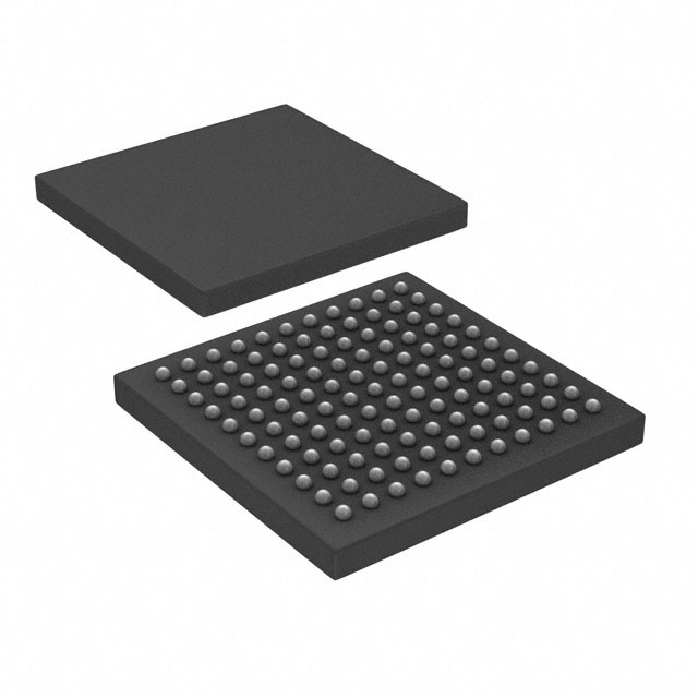
– 121-ball, 10- × 10-mm, 0.8-mm pitch Pb-free ball grid array (BGA)
– See Table 24 for details on the seven FX3 variants
• EZ-USB® software development kit (SDK) for code development of firmware and PC Applications
– Includes RTOS Framework (using ThreadX Version 5)
– Firmware examples covering all I/O modules
– Visual Studio host examples using C++ and C#
• SuperSpeed explorer board available for rapid prototyping
– Several accessory boards also available:
• Adapter boards for Xilinx/Altera FPGA development
• Adapter board for video development
• CPLD board for concept testing and initial development


