


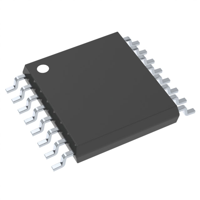
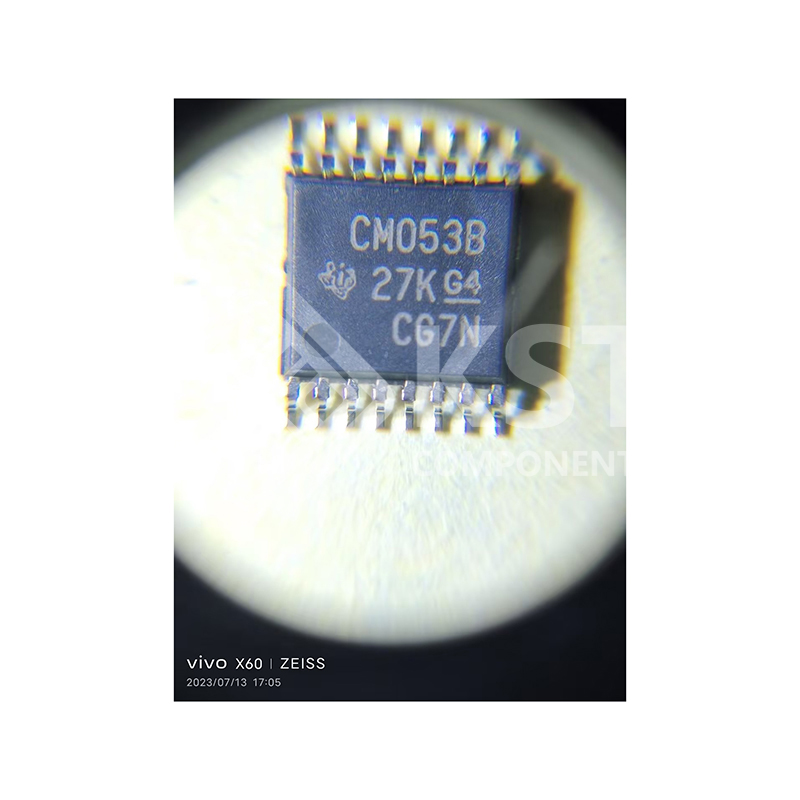
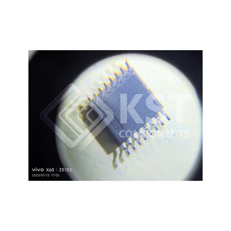
CD4053BPW
INQUIRY ONLINE
• Wide range of digital and analog signal levels:
– Digital: 3 V to 20 V
– Analog: ≤ 20 VP-P
• Low ON resistance, 125 Ω (typical) over 15 VP-P
signal input range for VDD – VEE = 18 V
• High OFF resistance, channel leakage of
±100 pA (typical) at VDD – VEE = 18 V
• Logic-level conversion for digital addressing
signals of 3 V to 20 V (VDD – VSS = 3 V to 20
V) to switch analog signals to 20 VP-P (VDD – VEE
= 20 V) matched switch characteristics, rON = 5 Ω
(typical) for VDD – VEE = 15 V very low quiescent
power dissipation under all digital-control input and
supply conditions, 0.2 µW (typical) at
VDD – VSS = VDD – VEE = 10 V
• Binary address decoding on chip
• 5 V, 10 V, and 15 V parametric ratings
• 100% tested for quiescent current at 20 V
• Maximum input current of 1 µA at 18 V over full
package temperature range, 100 nA at 18 V and
25°C
• Break-before-make switching eliminates channel
overlap