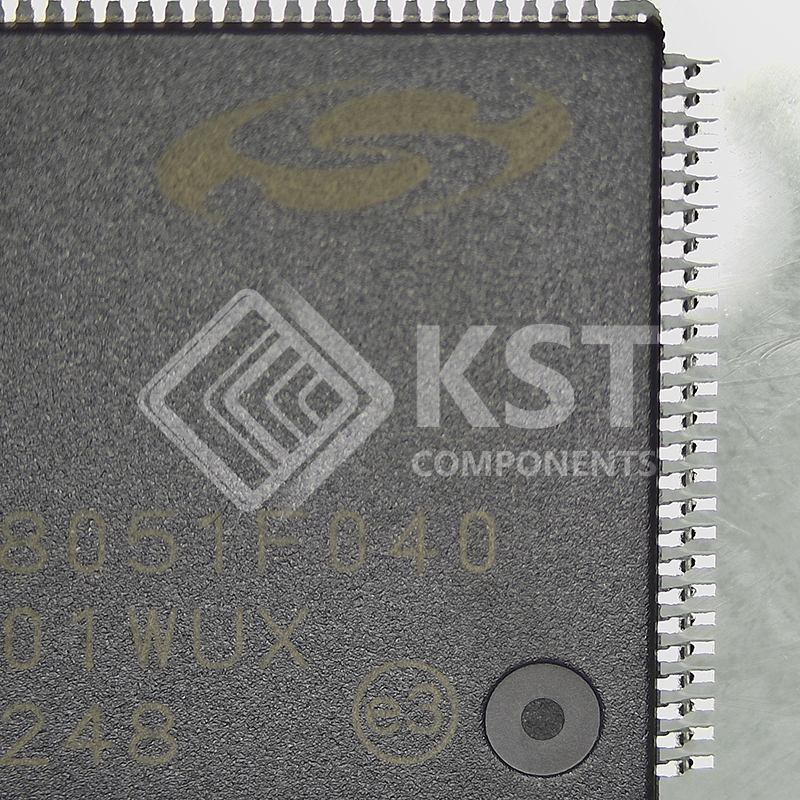
C8051F040-GQR

The C8051F04x family of devices are fully integrated mixed-signal System-on-a-Chip MCUs with 64 digital
I/O pins (C8051F040/2/4/6) or 32 digital I/O pins (C8051F041/3/5/7), and an integrated CAN 2.0B controller. Highlighted features are listed below; refer to Table 1.1 for specific product feature selection.
• High-Speed pipelined 8051-compatible CIP-51 microcontroller core (up to 25 MIPS)
• Controller Area Network (CAN 2.0B) Controller with 32 message objects, each with its own indentifier
mask.
• In-system, full-speed, non-intrusive debug interface (on-chip)
• True 12-bit (C8051F040/1) or 10-bit (C8051F042/3/4/5/6/7) 100 ksps 8-channel ADC with PGA and
analog multiplexer
• High Voltage Difference Amplifier input to the 12/10-bit ADC (60 V Peak-to-Peak) with programmable
gain.
• True 8-bit 500 ksps 8-channel ADC with PGA and analog multiplexer (C8051F040/1/2/3)
• Two 12-bit DACs with programmable update scheduling (C8051F040/1/2/3)
• 64 kB (C8051F040/1/2/3/4/5) or 32 kB (C8051F046/7) of in-system programmable Flash memory
• 4352 (4096 + 256) bytes of on-chip RAM
• External Data Memory Interface with 64 kB address space
• SPI, SMBus/I2C, and (2) UART serial interfaces implemented in hardware
• Five general purpose 16-bit Timers
• Programmable Counter/Timer Array with six capture/compare modules
• On-chip Watchdog Timer, VDD Monitor, and Temperature Sensor
With on-chip VDD monitor, Watchdog Timer, and clock oscillator, the C8051F04x family of devices are truly
stand-alone System-on-a-Chip solutions. All analog and digital peripherals are enabled/disabled and configured by user firmware. The Flash memory can be reprogrammed even in-circuit, providing non-volatile
data storage, and also allowing field upgrades of the 8051 firmware.
On-board JTAG debug circuitry allows non-intrusive (uses no on-chip resources), full speed, in-circuit programming and debugging using the production MCU installed in the final application. This debug system
supports inspection and modification of memory and registers, setting breakpoints, watchpoints, single
stepping, Run, and Halt commands. All analog and digital peripherals are fully functional while debugging
using JTAG.
Each MCU is specified for 2.7 V to 3.6 V operation over the industrial temperature range (–45 to +85 °C).
The Port I/Os, /RST, and JTAG pins are tolerant for input signals up to 5 V. The C8051F040/2/4/6 are available in a 100-pin TQFP and the C8051F041/3/5/7 are available in a 64-pin TQFP.


Download Details PDF

Notice:

In stock will ship in 2 days. Real-time inventory pls confirm with us.

INQUIRY ONLINE


    SPECIFICATION

    Analog Peripherals
    – 10 or 12-Bit SAR ADC
    • 12-bit (C8051F040/1) or
    10-bit (C8051F042/3/4/5/6/7) resolution
    • ± 1 LSB INL, guaranteed no missing codes
    • Programmable throughput up to 100 ksps
    • 13 External Inputs; single-ended or differential
    • SW programmable high voltage difference amplifier
    • Programmable amplifier gain: 16, 8, 4, 2, 1, 0.5
    • Data-dependent windowed interrupt generator
    • Built-in temperature sensor
    – 8-bit SAR ADC (C8051F040/1/2/3 only)
    • Programmable throughput up to 500 ksps
    • 8 External Inputs, single-ended or differential
    • Programmable amplifier gain: 4, 2, 1, 0.5
    – Two 12-bit DACs (C8051F040/1/2/3 only)
    • Can synchronize outputs to timers for jitter-free waveform generation
    – Three Analog Comparators
    • Programmable hysteresis/response time
    – Voltage Reference
    – Precision VDD Monitor/Brown-Out Detector
    On-Chip JTAG Debug & Boundary Scan
    – On-chip debug circuitry facilitates full- speed, nonintrusive in-circuit/in-system debugging
    – Provides breakpoints, single-stepping, watchpoints,
    stack monitor; inspect/modify memory and registers
    – Superior performance to emulation systems using
    ICE-chips, target pods, and sockets
    – IEEE1149.1 compliant boundary scan
    – Complete development kit
    High-Speed 8051 μC Core
    – Pipelined instruction architecture; executes 70% of
    instruction set in 1 or 2 system clocks
    – Up to 25 MIPS throughput with 25 MHz clock
    – 20 vectored interrupt sources
    Memory
    – 4352 bytes internal data RAM (4 k + 256)
    – 64 kB (C8051F040/1/2/3/4/5)
    or 32 kB (C8051F046/7) Flash; in-system programmable in 512-byte sectors
    – External 64 kB data memory interface (programmable multiplexed or non-multiplexed modes)
    Digital Peripherals
    – 8 byte-wide port I/O (C8051F040/2/4/6); 5 V tolerant
    – 4 byte-wide port I/O (C8051F041/3/5/7); 5 V tolerant
    – Bosch Controller Area Network (CAN 2.0B), hardware SMBus™ (I2C™ Compatible), SPI™, and
    two UART serial ports available concurrently
    – Programmable 16-bit counter/timer array with
    6 capture/compare modules
    – 5 general purpose 16-bit counter/timers
    – Dedicated watch-dog timer; bi-directional reset pin
    Clock Sources
    – Internal calibrated programmable oscillator: 3 to
    24.5 MHz
    – External oscillator: crystal, RC, C, or clock
    – Real-time clock mode using Timer 2, 3, 4, or PCA
    Supply Voltage: 2.7 to 3.6 V
    – Multiple power saving sleep and shutdown modes
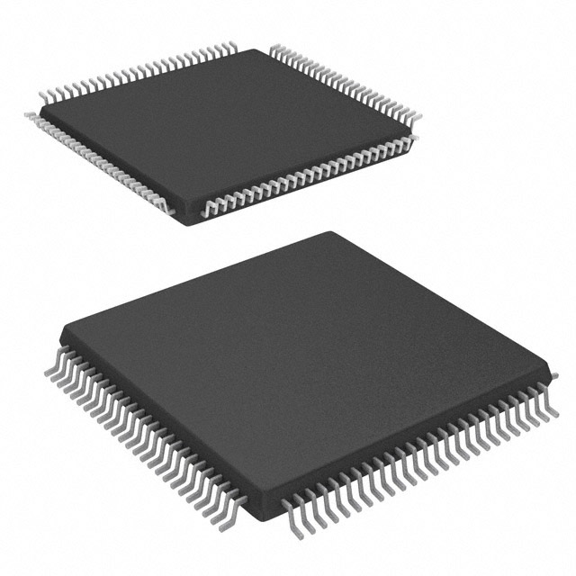
    100-Pin and 64-Pin TQFP Packages Available
    – Temperature Range: –40 to +85 °C