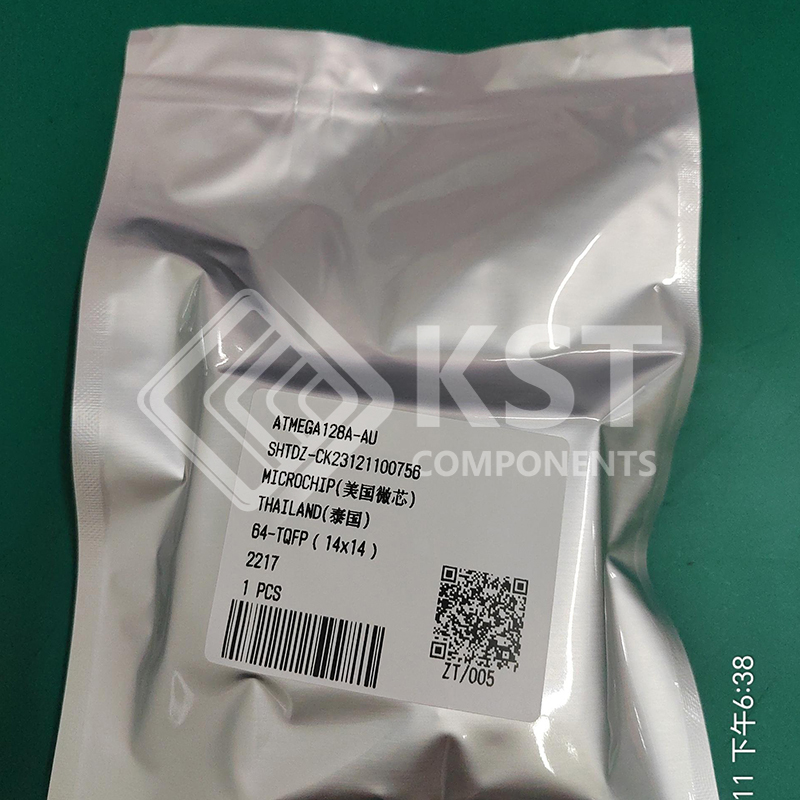
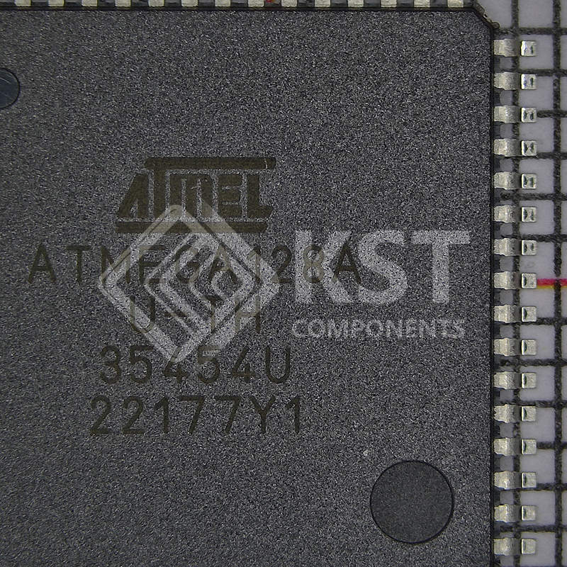
ATMEGA128A-AU

The Atmel AVR core combines a rich instruction set with 32 general purpose working registers. All the 32
registers are directly connected to the Arithmetic Logic Unit (ALU), allowing two independent registers to
be accessed in one single instruction executed in one clock cycle. The resulting architecture is more code
efficient while achieving throughputs up to ten times faster than conventional CISC microcontrollers.
The ATmega128A provides the following features: 128Kbytes of In-System Programmable Flash with
Read- While-Write capabilities, 4Kbytes EEPROM, 4Kbytes SRAM, 53 general purpose I/O lines, 32
general purpose working registers, Real Time Counter (RTC), four flexible Timer/Counters with compare
modes and PWM, 2 USARTs, one byte oriented Two-wire Serial Interface, an 8-channel, 10-bit ADC with
optional differential input stage with programmable gain, programmable Watchdog Timer with Internal
Oscillator, one SPI serial port, IEEE std. 1149.1 compliant JTAG test interface, also used for accessing
the On-chip Debug system and programming and six software selectable power saving modes. The Idle
mode stops the CPU while allowing the SRAM, Timer/Counters, SPI port, and interrupt system to
continue functioning. The Power-down mode saves the register contents but freezes the Oscillator,
disabling all other chip functions until the next interrupt or Hardware Reset. In Power-save mode, the
asynchronous timer continues to run, allowing the user to maintain a timer base while the rest of the
device is sleeping. The ADC Noise Reduction mode stops the CPU and all I/O modules except
Asynchronous Timer and ADC, to minimize switching noise during ADC conversions. In Standby mode,
the Crystal/Resonator Oscillator is running while the rest of the device is sleeping. This allows very fast
start-up combined with low power consumption. In Extended Standby mode, both the main Oscillator and
the Asynchronous Timer continue to run.
The device is manufactured using Atmel’s high-density nonvolatile memory technology. The On-chip ISP
Flash allows the program memory to be reprogrammed in-system through an SPI serial interface, by a
conventional nonvolatile memory programmer, or by an On-chip Boot program running on the AVR core.
The boot program can use any interface to download the application program in the application Flash
memory. Software in the Boot Flash section will continue to run while the Application Flash section is
updated, providing true Read- While-Write operation. By combining an 8-bit RISC CPU with In-System
Self-Programmable Flash on a monolithic chip, the Atmel ATmega128A is a powerful microcontroller that
provides a highly flexible and cost effective solution to many embedded control application
The ATmega128A AVR is supported with a full suite of program and system development tools including:
C compilers, macro assemblers, program debugger/simulators, in-circuit emulators, and evaluation kits.


Download Details PDF

Notice:

In stock will ship in 2 days. Real-time inventory pls confirm with us.

INQUIRY ONLINE


    SPECIFICATION

    • High-performance, Low-power Atmel AVR 8-bit Microcontroller
    • Advanced RISC Architecture
    – 133 Powerful Instructions – Most Single-clock Cycle Execution
    – 32 × 8 General Purpose Working Registers + Peripheral Control
    Registers
    – Fully Static Operation
    – Up to 16MIPS Throughput at 16MHz
    – On-chip 2-cycle Multiplier
    • High Endurance Non-volatile Memory segments
    – 128Kbytes of In-System Self-programmable Flash program
    memory
    – 4Kbytes EEPROM
    – 4Kbytes Internal SRAM
    – Write/Erase cycles: 10,000 Flash/100,000 EEPROM
    – Data retention: 20 years at 85°C/100 years at 25°C(1)
    – Optional Boot Code Section with Independent Lock Bits
    • In-System Programming by On-chip Boot Program
    • True Read-While-Write Operation
    – Up to 64 Kbytes Optional External Memory Space
    – Programming Lock for Software Security
    – SPI Interface for In-System Programming
    • JTAG (IEEE std. 1149.1 Compliant) Interface
    – Boundary-scan Capabilities According to the JTAG Standard
    – Extensive On-chip Debug Support

    – Programming of Flash, EEPROM, Fuses and Lock Bits through the JTAG Interface
    • Atmel QTouch® library support
    – Capacitive touch buttons, sliders and wheels
    – Atmel QTouch and QMatrix acquisition
    – Up to 64 sense channels
    • Peripheral Features
    – Two 8-bit Timer/Counters with Separate Prescalers and Compare Modes
    – Two Expanded 16-bit Timer/Counters with Separate Prescaler, Compare Mode and Capture
    Mode
    – Real Time Counter with Separate Oscillator
    – Two 8-bit PWM Channels
    – 6 PWM Channels with Programmable Resolution from 2 to 16 Bits
    – Output Compare Modulator
    – 8-channel, 10-bit ADC
    • 8 Single-ended Channels
    • 7 Differential Channels
    • 2 Differential Channels with Programmable Gain at 1x, 10x, or 200x
    – Byte-oriented Two-wire Serial Interface
    – Dual Programmable Serial USARTs
    – Master/Slave SPI Serial Interface
    – Programmable Watchdog Timer with On-chip Oscillator
    – On-chip Analog Comparator
    • Special Microcontroller Features
    – Power-on Reset and Programmable Brown-out Detection
    – Internal Calibrated RC Oscillator
    – External and Internal Interrupt Sources
    – Six Sleep Modes: Idle, ADC Noise Reduction, Power-save, Power-down, Standby, and
    Extended Standby
    – Software Selectable Clock Frequency
    – ATmega103 Compatibility Mode Selected by a Fuse
    – Global Pull-up Disable
    • I/O and Packages
    – 53 Programmable I/O Lines
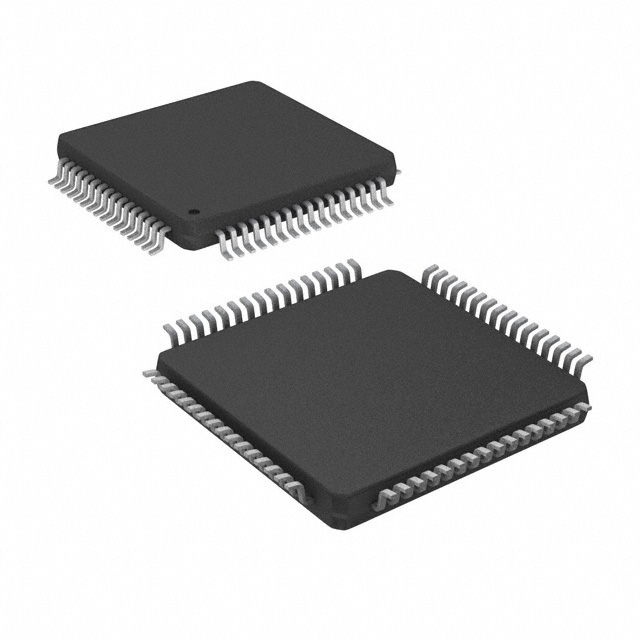
    – 64-lead TQFP and 64-pad QFN/MLF
    • Operating Voltages
    – 2.7 – 5.5V
    • Speed Grades
    – 0 – 16MHz