


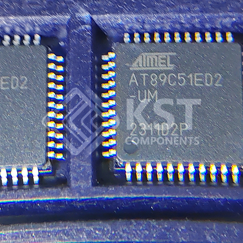
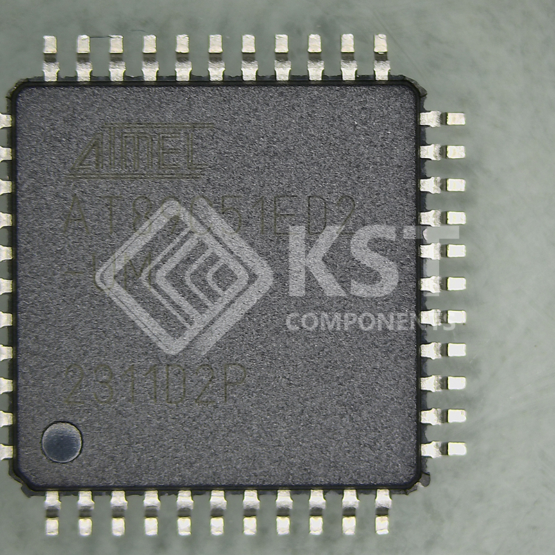
AT89C51ED2-RLTUM
INQUIRY ONLINE
• 80C52 Compatible
– 8051 Instruction Compatible
– Six 8-bit I/O Ports (64 Pins or 68 Pins Versions)
– Four 8-bit I/O Ports (44 Pins Version)
– Three 16-bit Timer/Counters
– 256 Bytes Scratch Pad RAM
– 9 Interrupt Sources with 4 Priority Levels
• Integrated Power Monitor (POR/PFD) to Supervise Internal Power Supply
• ISP (In-System Programming) Using Standard VCC Power Supply
• 2048 Bytes Boot ROM Contains Low Level Flash Programming Routines and a Default
Serial Loader
• High-speed Architecture
– In Standard Mode:
• 40 MHz (Vcc 2.7V to 5.5V, both Internal and external code execution)
• 60 MHz (Vcc 4.5V to 5.5V and Internal Code execution only)
– In X2 mode (6 Clocks/machine cycle)
• 20 MHz (Vcc 2.7V to 5.5V, both Internal and external code execution)
• 30 MHz (Vcc 4.5V to 5.5V and Internal Code execution only)
• 64K Bytes On-chip Flash Program/Data Memory
– Byte and Page (128 Bytes) Erase and Write
– 100k Write Cycles
• On-chip 1792 bytes Expanded RAM (XRAM)
– Software Selectable Size (0, 256, 512, 768, 1024, 1792 Bytes)
– 768 Bytes Selected at Reset for T89C51RD2 Compatibility
• On-chip 2048 Bytes EEPROM Block for Data Storage (AT89C51ED2 Only)
• 100K Write Cycles
• Dual Data Pointer
• Variable Length MOVX for Slow RAM/Peripherals
• Improved X2 Mode with Independent Selection for CPU and Each Peripheral
• Keyboard Interrupt Interface on Port 1
• SPI Interface (Master/Slave Mode)
• 8-bit Clock Prescaler
• 16-bit Programmable Counter Array
– High Speed Output
– Compare/Capture
– Pulse Width Modulator
– Watchdog Timer Capabilities
• Asynchronous Port Reset
• Full-duplex Enhanced UART with Dedicated Internal Baud Rate Generator
• Low EMI (Inhibit ALE)
• Hardware Watchdog Timer (One-time Enabled with Reset-Out), Power-off Flag
• Power Control Modes: Idle Mode, Power-down Mode
• Single Range Power Supply: 2.7V to 5.5V
• Industrial Temperature Range (-40 to +85°C)
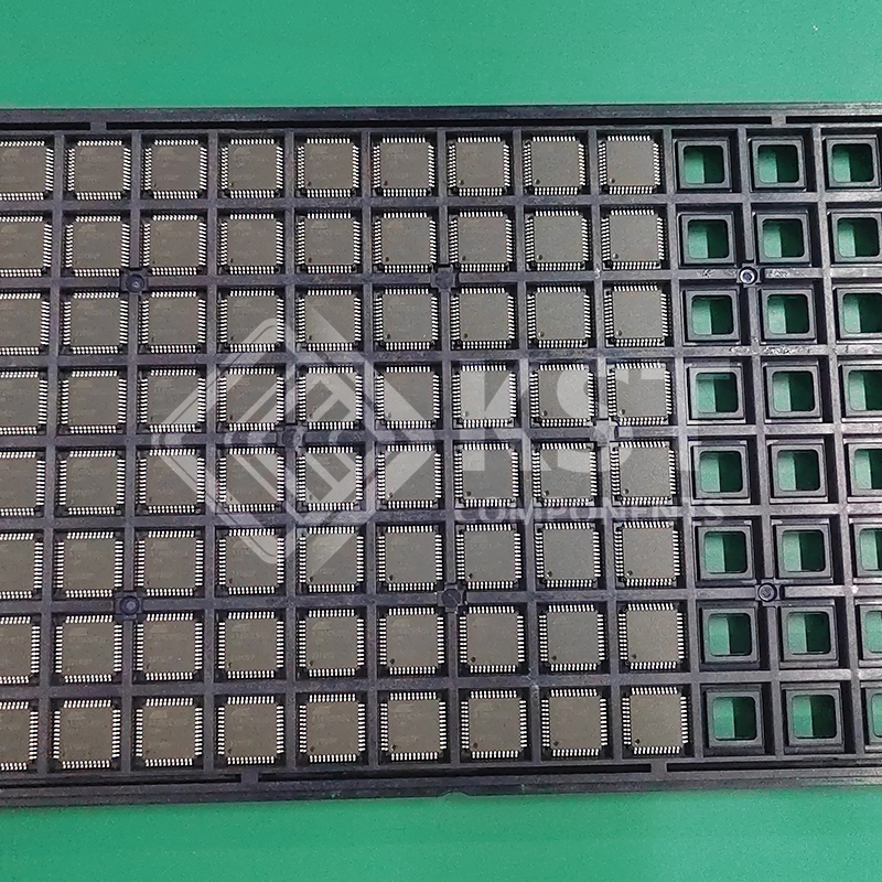
• Packages: PLCC44, VQFP44, PLCC68, VQFP64