


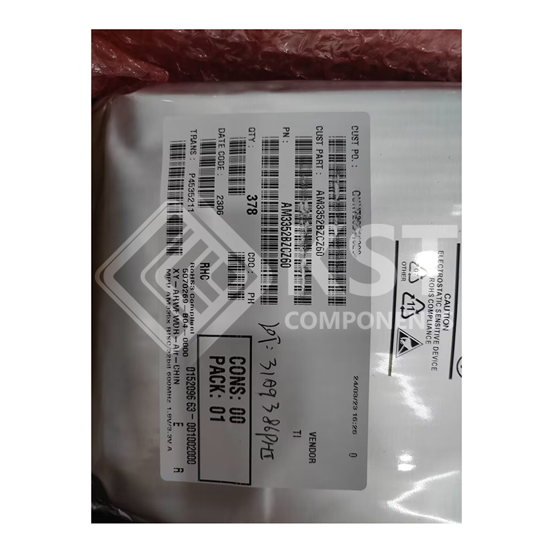
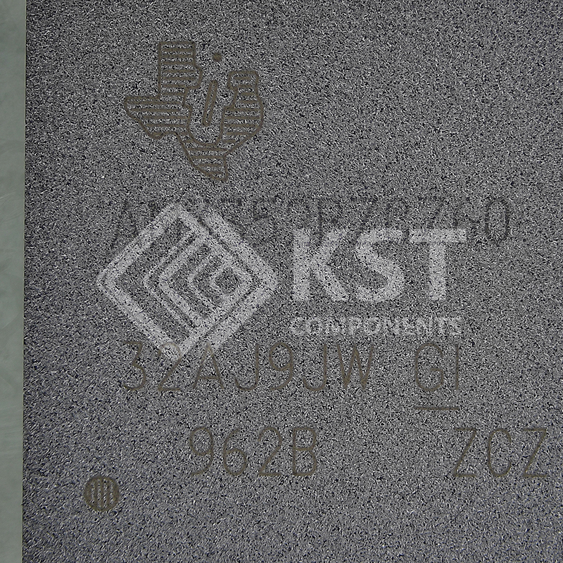

AM3352BZCZ60
INQUIRY ONLINE
• Up to 1-GHz Sitara™ ARM® Cortex®
-A8 32‑Bit
RISC Processor
– NEON™ SIMD Coprocessor
– 32KB of L1 Instruction and 32KB of Data Cache
With Single-Error Detection (Parity)
– 256KB of L2 Cache With Error Correcting Code
(ECC)
– 176KB of On-Chip Boot ROM
– 64KB of Dedicated RAM
– Emulation and Debug – JTAG
– Interrupt Controller (up to 128 Interrupt
Requests)
• On-Chip Memory (Shared L3 RAM)
– 64KB of General-Purpose On-Chip Memory
Controller (OCMC) RAM
– Accessible to All Masters
– Supports Retention for Fast Wakeup
• External Memory Interfaces (EMIF)
– mDDR(LPDDR), DDR2, DDR3, DDR3L
Controller:
– mDDR: 200-MHz Clock (400-MHz Data Rate)
– DDR2: 266-MHz Clock (532-MHz Data Rate)
– DDR3: 400-MHz Clock (800-MHz Data Rate)
– DDR3L: 400-MHz Clock (800-MHz Data
Rate)
– 16-Bit Data Bus
– 1GB of Total Addressable Space
– Supports One x16 or Two x8 Memory Device
Configurations
– General-Purpose Memory Controller (GPMC)
– Flexible 8-Bit and 16-Bit Asynchronous
Memory Interface With up to Seven Chip
Selects (NAND, NOR, Muxed-NOR, SRAM)
– Uses BCH Code to Support 4-, 8-, or 16-Bit
ECC
– Uses Hamming Code to Support 1-Bit ECC
– Error Locator Module (ELM)
– Used in Conjunction With the GPMC to
Locate Addresses of Data Errors from
Syndrome Polynomials Generated Using a
BCH Algorithm
– Supports 4-, 8-, and 16-Bit per 512-Byte
Block Error Location Based on BCH
Algorithms
• Programmable Real-Time Unit Subsystem and
Industrial Communication Subsystem (PRU-ICSS)
– Supports Protocols such as EtherCAT®
,
PROFIBUS, PROFINET, EtherNet/IP™, and
More
– Two Programmable Real-Time Units (PRUs)
– 32-Bit Load/Store RISC Processor Capable
of Running at 200 MHz
– 8KB of Instruction RAM With Single-Error
Detection (Parity)
– 8KB of Data RAM With Single-Error Detection
(Parity)
– Single-Cycle 32-Bit Multiplier With 64-Bit
Accumulator
– Enhanced GPIO Module Provides ShiftIn/Out Support and Parallel Latch on External
Signal
– 12KB of Shared RAM With Single-Error
Detection (Parity)
– Three 120-Byte Register Banks Accessible by
Each PRU
– Interrupt Controller (INTC) for Handling System
Input Events
– Local Interconnect Bus for Connecting Internal
and External Masters to the Resources Inside
the PRU-ICSS
– Peripherals Inside the PRU-ICSS:
– One UART Port With Flow Control Pins,
Supports up to 12 Mbps
– One Enhanced Capture (eCAP) Module
– Two MII Ethernet Ports that Support Industrial
Ethernet, such as EtherCAT
– One MDIO Port
• Power, Reset, and Clock Management (PRCM)
Module
– Controls the Entry and Exit of Stand-By and
Deep-Sleep Modes
– Responsible for Sleep Sequencing, Power
Domain Switch-Off Sequencing, Wake-Up
Sequencing, and Power Domain Switch-On
Sequencing
– Clocks
– Integrated 15- to 35-MHz High-Frequency
Oscillator Used to Generate a Reference
Clock for Various System and Peripheral
Clocks
– Supports Individual Clock Enable and Disable
Control for Subsystems and Peripherals to
Facilitate Reduced Power Consumption
– Five ADPLLs to Generate System Clocks
(MPU Subsystem, DDR Interface, USB and
Peripherals [MMC and SD, UART, SPI, I
2C], L3, L4, Ethernet, GFX [SGX530], LCD Pixel
Clock)
– Power
– Two Nonswitchable Power Domains (RealTime Clock [RTC], Wake-Up Logic
[WAKEUP])
– Three Switchable Power Domains (MPU
Subsystem [MPU], SGX530 [GFX],
Peripherals and Infrastructure [PER])
– Implements SmartReflex™ Class 2B for Core
Voltage Scaling Based On Die Temperature,
Process Variation, and Performance
(Adaptive Voltage Scaling [AVS])
– Dynamic Voltage Frequency Scaling (DVFS)
• Real-Time Clock (RTC)
– Real-Time Date (Day-Month-Year-Day of Week)
and Time (Hours-Minutes-Seconds) Information
– Internal 32.768-kHz Oscillator, RTC Logic and
1.1-V Internal LDO
– Independent Power-on-Reset
(RTC_PWRONRSTn) Input
– Dedicated Input Pin (EXT_WAKEUP) for
External Wake Events
– Programmable Alarm Can be Used to Generate
Internal Interrupts to the PRCM (for Wakeup) or
Cortex-A8 (for Event Notification)
– Programmable Alarm Can be Used With
External Output (PMIC_POWER_EN) to Enable
the Power Management IC to Restore Non-RTC
Power Domains
• Peripherals
– Up to Two USB 2.0 High-Speed DRD (DualRole Device) Ports With Integrated PHY
– Up to Two Industrial Gigabit Ethernet MACs (10,
100, 1000 Mbps)
– Integrated Switch
– Each MAC Supports MII, RMII, RGMII, and
MDIO Interfaces
– Ethernet MACs and Switch Can Operate
Independent of Other Functions
– IEEE 1588v1 Precision Time Protocol (PTP)
– Up to Two Controller-Area Network (CAN) Ports
– Supports CAN Version 2 Parts A and B
– Up to Two Multichannel Audio Serial Ports
(McASPs)
– Transmit and Receive Clocks up to 50 MHz
– Up to Four Serial Data Pins per McASP Port
With Independent TX and RX Clocks
– Supports Time Division Multiplexing (TDM),
Inter-IC Sound (I2S), and Similar Formats
– Supports Digital Audio Interface Transmission
(SPDIF, IEC60958-1, and AES-3 Formats)
– FIFO Buffers for Transmit and Receive (256
Bytes)
– Up to Six UARTs
– All UARTs Support IrDA and CIR Modes
– All UARTs Support RTS and CTS Flow
Control
– UART1 Supports Full Modem Control
– Up to Two Master and Slave McSPI Serial
Interfaces
– Up to Two Chip Selects
– Up to 48 MHz
– Up to Three MMC, SD, SDIO Ports
– 1-, 4- and 8-Bit MMC, SD, SDIO Modes
– MMCSD0 has Dedicated Power Rail for 1.8‑V
or 3.3-V Operation
– Up to 48-MHz Data Transfer Rate
– Supports Card Detect and Write Protect
– Complies With MMC4.3, SD, SDIO 2.0
Specifications
– Up to Three I
2C Master and Slave Interfaces
– Standard Mode (up to 100 kHz)
– Fast Mode (up to 400 kHz)
– Up to Four Banks of General-Purpose I/O
(GPIO) Pins
– 32 GPIO Pins per Bank (Multiplexed With
Other Functional Pins)
– GPIO Pins Can be Used as Interrupt Inputs
(up to Two Interrupt Inputs per Bank)
– Up to Three External DMA Event Inputs that can
Also be Used as Interrupt Inputs
– Eight 32-Bit General-Purpose Timers
– DMTIMER1 is a 1-ms Timer Used for
Operating System (OS) Ticks
– DMTIMER4–DMTIMER7 are Pinned Out
– One Watchdog Timer
– SGX530 3D Graphics Engine
– Tile-Based Architecture Delivering up to 20
Million Polygons per Second
– Universal Scalable Shader Engine (USSE) is
a Multithreaded Engine Incorporating Pixel
and Vertex Shader Functionality
– Advanced Shader Feature Set in Excess of
Microsoft VS3.0, PS3.0, and OGL2.0
– Industry Standard API Support of Direct3D
Mobile, OGL-ES 1.1 and 2.0, and OpenMax
– Fine-Grained Task Switching, Load
Balancing, and Power Management
– Advanced Geometry DMA-Driven Operation
for Minimum CPU Interaction
– Programmable High-Quality Image AntiAliasing
– Fully Virtualized Memory Addressing for OS
Operation in a Unified Memory Architecture
– LCD Controller
– Up to 24-Bit Data Output; 8 Bits per Pixel
(RGB)
– Resolution up to 2048 × 2048 (With
Maximum 126-MHz Pixel Clock)
– Integrated LCD Interface Display Driver
(LIDD) Controller
– Integrated Raster Controller
– Integrated DMA Engine to Pull Data from the
External Frame Buffer Without Burdening the
Processor via Interrupts or a Firmware Timer
– 512-Word Deep Internal FIFO
– Supported Display Types:
– Character Displays – Uses LIDD Controller
to Program these Displays
– Passive Matrix LCD Displays – Uses LCD
Raster Display Controller to Provide
Timing and Data for Constant Graphics
Refresh to a Passive Display
– Active Matrix LCD Displays – Uses
External Frame Buffer Space and the
Internal DMA Engine to Drive Streaming
Data to the Panel
– 12-Bit Successive Approximation Register
(SAR) ADC
– 200K Samples per Second
– Input can be Selected from any of the Eight
Analog Inputs Multiplexed Through an 8:1
Analog Switch
– Can be Configured to Operate as a 4-Wire, 5-
Wire, or 8-Wire Resistive Touch Screen
Controller (TSC) Interface
– Up to Three 32-Bit eCAP Modules
– Configurable as Three Capture Inputs or
Three Auxiliary PWM Outputs
– Up to Three Enhanced High-Resolution PWM
Modules (eHRPWMs)
– Dedicated 16-Bit Time-Base Counter With
Time and Frequency Controls
– Configurable as Six Single-Ended, Six DualEdge Symmetric, or Three Dual-Edge
Asymmetric Outputs
– Up to Three 32-Bit Enhanced Quadrature
Encoder Pulse (eQEP) Modules
• Device Identification
– Contains Electrical Fuse Farm (FuseFarm) of
Which Some Bits are Factory Programmable
– Production ID
– Device Part Number (Unique JTAG ID)
– Device Revision (Readable by Host ARM)
• Debug Interface Support
– JTAG and cJTAG for ARM (Cortex-A8 and
PRCM), PRU-ICSS Debug
– Supports Device Boundary Scan
– Supports IEEE 1500
• DMA
– On-Chip Enhanced DMA Controller (EDMA) has
Three Third-Party Transfer Controllers (TPTCs)
and One Third-Party Channel Controller
(TPCC), Which Supports up to 64
Programmable Logical Channels and Eight
QDMA Channels. EDMA is Used for:
– Transfers to and from On-Chip Memories
– Transfers to and from External Storage
(EMIF, GPMC, Slave Peripherals)
• Inter-Processor Communication (IPC)
– Integrates Hardware-Based Mailbox for IPC and
Spinlock for Process Synchronization Between
Cortex-A8, PRCM, and PRU-ICSS
– Mailbox Registers that Generate Interrupts
– Four Initiators (Cortex-A8, PRCM, PRU0,
PRU1)
– Spinlock has 128 Software-Assigned Lock
Registers
• Security
– Crypto Hardware Accelerators (AES, SHA,
RNG)
– Secure Boot (optional; requires custom part
engagement with TI)
• Boot Modes
– Boot Mode is Selected Through Boot
Configuration Pins Latched on the Rising Edge
of the PWRONRSTn Reset Input Pin
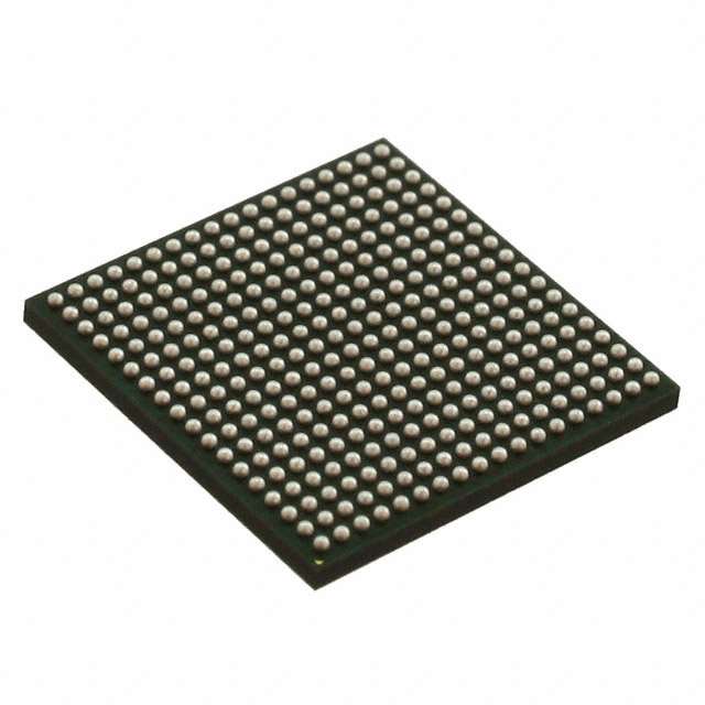
• Packages:
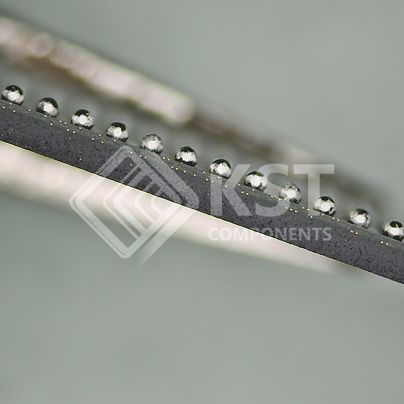
– 298-Pin S-PBGA-N298 Via Channel Package
(ZCE Suffix), 0.65-mm Ball Pitch
– 324-Pin S-PBGA-N324 Package
(ZCZ Suffix), 0.80-mm Ball Pitch