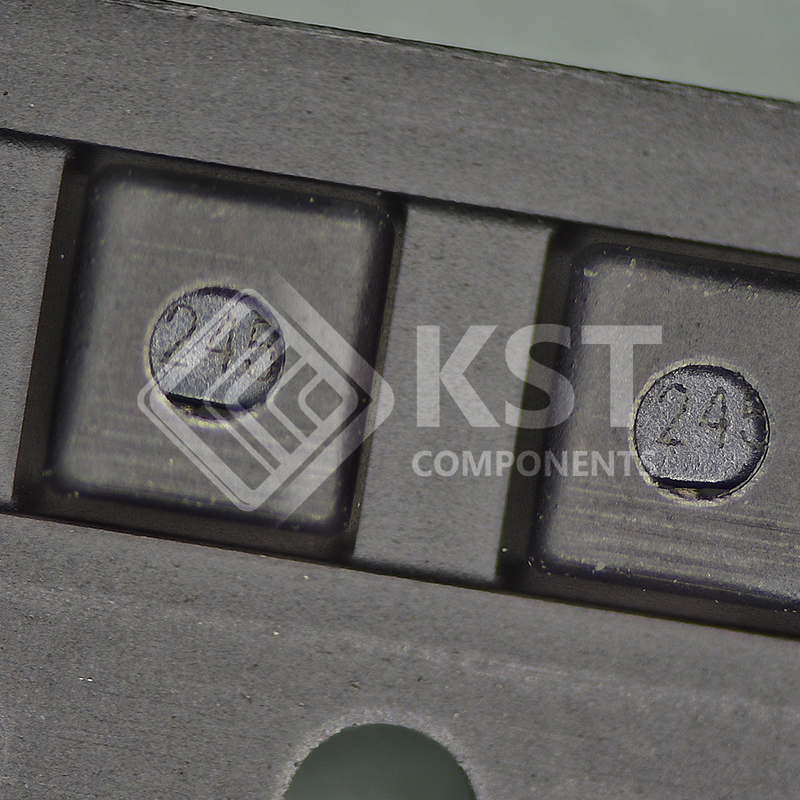
ADCMP601BKSZ

The ADCMP600, ADCMP601, and ADCMP602 are very fast
comparators fabricated on XFCB2, an Analog Devices, Inc.
proprietary process. These comparators are exceptionally
versatile and easy to use. Features include an input range from
GND − 0.5 V to VCC + 0.2 V, low noise, TTL-/CMOS-compatible
output drivers, and latch inputs with adjustable hysteresis
and/or shutdown inputs.
The device offers 5 ns propagation delay with 10 mV overdrive
on 3 mA typical supply current.
A flexible power supply scheme allows the devices to operate
with a single +2.5 V positive supply and a −0.5 V to +2.8 V
input signal range up to a +5.5 V positive supply with a −0.5 V
to +5.8 V input signal range. Split input/output supplies with no
sequencing restrictions on the ADCMP602 support a wide
input signal range while still allowing independent output
swing control and power savings.
The TTL-/CMOS-compatible output stage is designed to drive
up to 5 pF with full timing specs and to degrade in a graceful
and linear fashion as additional capacitance is added. The
comparator input stage offers robust protection against large
input overdrive, and the outputs do not phase reverse when the
valid input signal range is exceeded. Latch and programmable
hysteresis features are also provided with a unique single-pin
control option.
The ADCMP600 is available in 5-lead SC70 and SOT-23
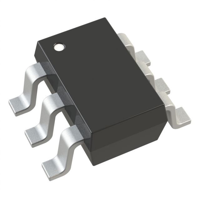
packages, the ADCMP601 is available in a 6-lead SC70 package,
and the ADCMP602 is available in an 8-lead MSOP package.

Category:

Download Details PDF

Notice:

In stock will ship in 2 days. Real-time inventory pls confirm with us.

INQUIRY ONLINE


    SPECIFICATION

    Fully specified rail to rail at VCC = 2.5 V to 5.5 V
    Input common-mode voltage from −0.2 V to VCC + 0.2 V
    Low glitch CMOS-/TTL-compatible output stage
    3.5 ns propagation delay
    10 mW at 3.3 V
    Shutdown pin
    Single-pin control for programmable hysteresis and latch
    Power supply rejection > 50 dB
    Improved replacement for MAX999
    −40°C to +125°C operation