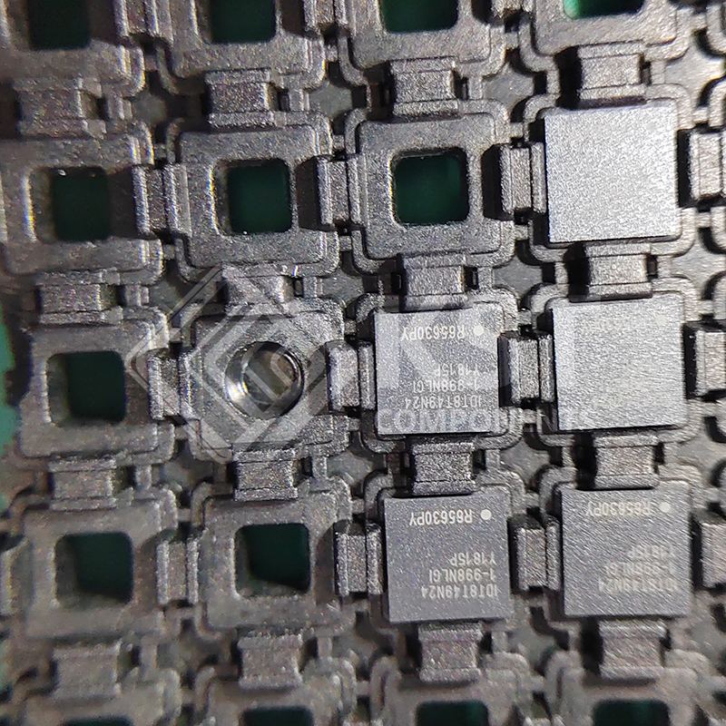
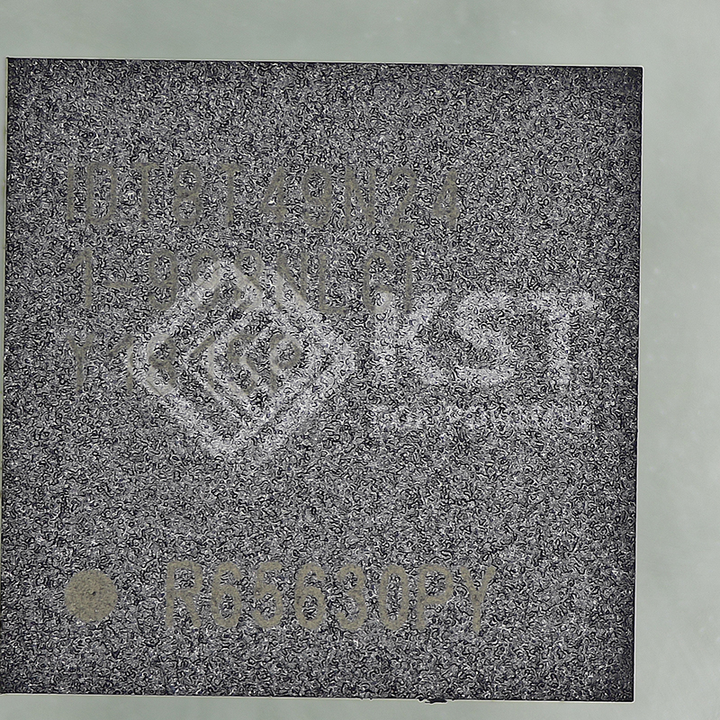
8T49N241-998NLGI

The 8T49N241 has one fractional-feedback PLL that can be used as
a jitter attenuator and frequency translator. It is equipped with one
integer and three fractional output dividers, allowing the generation of
up to four different output frequencies, ranging from 8kHz to 1GHz.
These frequencies are completely independent of each other, the
input reference frequencies, and the crystal reference frequency. The
device places virtually no constraints on input to output frequency
conversion, supporting all FEC rates, including the new revision of
ITU-T Recommendation G.709 (2009), most with 0ppm conversion
error. The outputs may select among LVPECL, LVDS, HCSL or
LVCMOS output levels.
This makes it ideal to be used in any frequency synthesis application,
including 1G, 10G, 40G and 100G Synchronous Ethernet, OTN, and
SONET/SDH, including ITU-T G.709 (2009) FEC rates.
The 8T49N241 accepts up to two differential or single-ended input
clocks and a fundamental-mode crystal input. The internal PLL can
lock to either of the input reference clocks or just to the crystal to
behave as a frequency synthesizer. The PLL can use the second
input for redundant backup of the primary input reference, but in this
case, both input clock references must be related in frequency.
The device supports hitless reference switching between input
clocks. The device monitors both input clocks for Loss of Signal
(LOS), and generates an alarm when an input clock failure is
detected. Automatic and manual hitless reference switching options
are supported. LOS behavior can be set to support gapped or
un-gapped clocks.
The 8T49N241 supports holdover. The holdover has an initial
accuracy of ±50ppB from the point where the loss of all applicable
input reference(s) has been detected. It maintains a historical
average operating point for the PLL that may be returned to in
holdover at a limited phase slope.
The PLL has a register-selectable loop bandwidth from 0.2Hz to
6.4kHz.
The device supports Output Enable & Clock Select inputs and Lock,
Holdover & LOS status outputs.
The device is programmable through an I2C interface. It also supports
I
2C master capability to allow the register configuration to be read
from an external EEPROM.
Programming with IDT’s Timing Commander software is
recommended for optimal device performance. Factory
pre-programmed devices are also available.

Category:

Download Details PDF

Notice:

In stock will ship in 2 days. Real-time inventory pls confirm with us.

INQUIRY ONLINE


    SPECIFICATION

    • Supports SDH/SONET and Synchronous Ethernet clocks including
    all FEC rate conversions
    • 0.35ps RMS Typical Jitter (including spurs): 12kHz to 20MHz
    • Operating Modes: Synthesizer, Jitter Attenuator
    • Operates from a 10MHz to 50MHz fundamental-mode crystal or a
    10MHz to 125MHz external oscillator
    • Initial holdover accuracy of +50ppb.
    • Accepts up to 2 LVPECL, LVDS, LVHSTL or LVCMOS input clocks
    • Accepts frequencies ranging from 8kHz to 875MHz
    • Auto and manual clock selection with hitless switching
    • Clock input monitoring including support for gapped clocks
    • Phase-slope limiting and fully hitless switching options to control
    output clock phase transients
    • Generates four LVPECL / LVDS / HCSL or eight LVCMOS output
    clocks
    • Output frequencies ranging from 8kHz up to 1.0GHz
    (differential)
    • Output frequencies ranging from 8kHz to 250MHz (LVCMOS)
    • One integer divider ranging from ÷4 to ÷786,420
    • Three fractional output dividers (see Output Dividers)
    • Programmable loop bandwidth settings from 0.2Hz to 6.4kHz
    • Optional fast-lock function
    • Four General Purpose I/O pins with optional support for status &
    control:
    • Two Output Enable control inputs provide control over the four
    clocks
    • Manual clock selection control input
    • Lock, Holdover and Loss-of-Signal alarm outputs
    • Open-drain Interrupt pin
    • Register programmable through I2C or via external I2C EEPROM
    • Full 2.5V or 3.3V supply modes, 1.8V support for LVCMOS outputs,
    GPIO and control pins
    • -40°C to 85°C ambient operating temperature
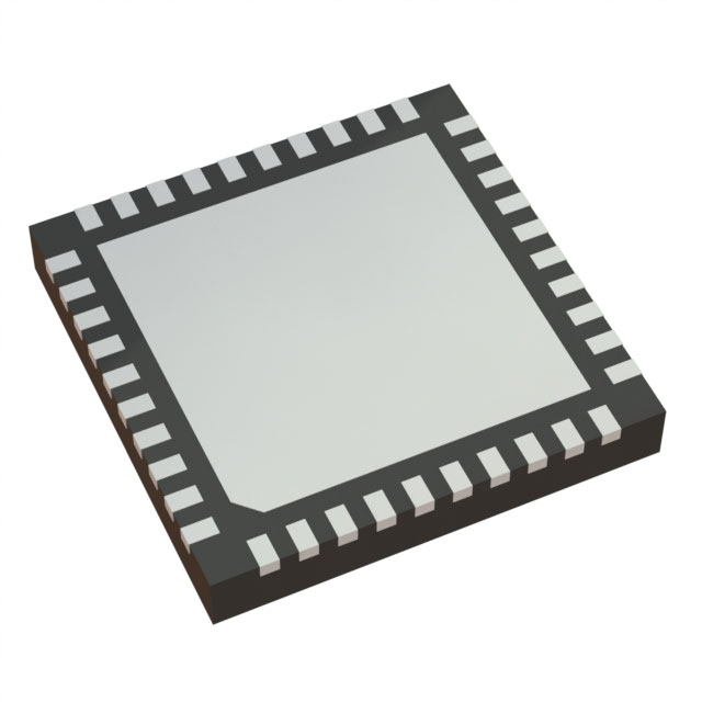
    • Package: 40-VFQFPN, lead-free (RoHS 6)