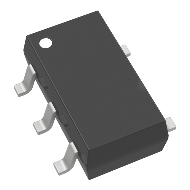
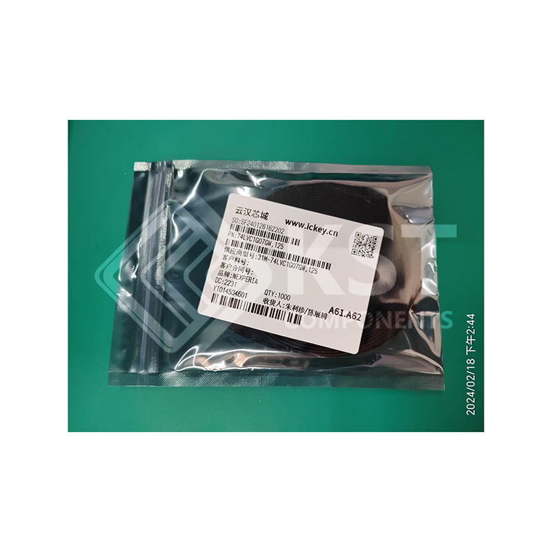
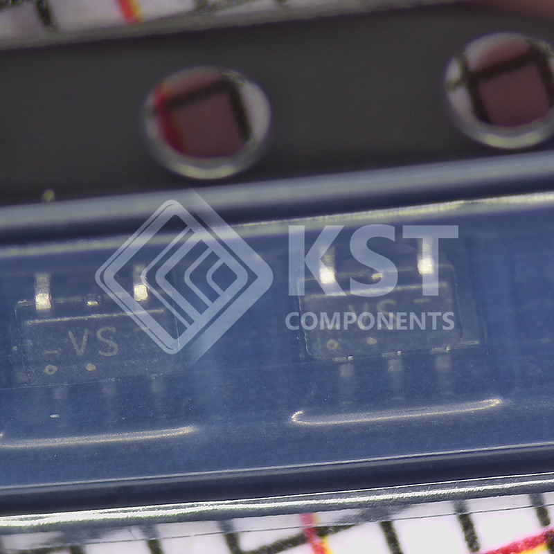
74LVC1G07GW,125

The 74LVC1G07 is a single buffer with open-drain output. Inputs can be driven from either 3.3 V
or 5 V devices. This feature allows the use of these devices as translators in mixed 3.3 V and 5 V
environments. Schmitt-trigger action at all inputs makes the circuit tolerant of slower input rise and
fall times. This device is fully specified for partial power down applications using IOFF. The IOFF
circuitry disables the output, preventing the potentially damaging backflow current through the
device when it is powered down.

Category:

Download Details PDF

Notice:

In stock will ship in 2 days. Real-time inventory pls confirm with us.

INQUIRY ONLINE


    SPECIFICATION

    • Wide supply voltage range from 1.65 V to 5.5 V
    • Overvoltage tolerant inputs to 5.5 V
    • High noise immunity
    • CMOS low power consumption
    • IOFF circuitry provides partial Power-down mode operation
    • -24 mA output drive (VCC = 3.0 V)
    • Latch-up performance exceeds 250 mA
    • Direct interface with TTL levels
    • Complies with JEDEC standard:
    • JESD8-7 (1.65 V to 1.95 V)
    • JESD8-5 (2.3 V to 2.7 V)
    • JESD8C (2.7 V to 3.6 V)
    • JESD36 (4.5 V to 5.5 V)
    • ESD protection:
    • HBM: ANSI/ESDA/JEDEC JS-001 class 2 exceeds 2000 V
    • CDM: ANSI/ESDA/JEDEC JS-002 class C3 exceeds 1000 V
    • Multiple package options
    • Specified from -40 °C to +85 °C and -40 °C to +125 °C