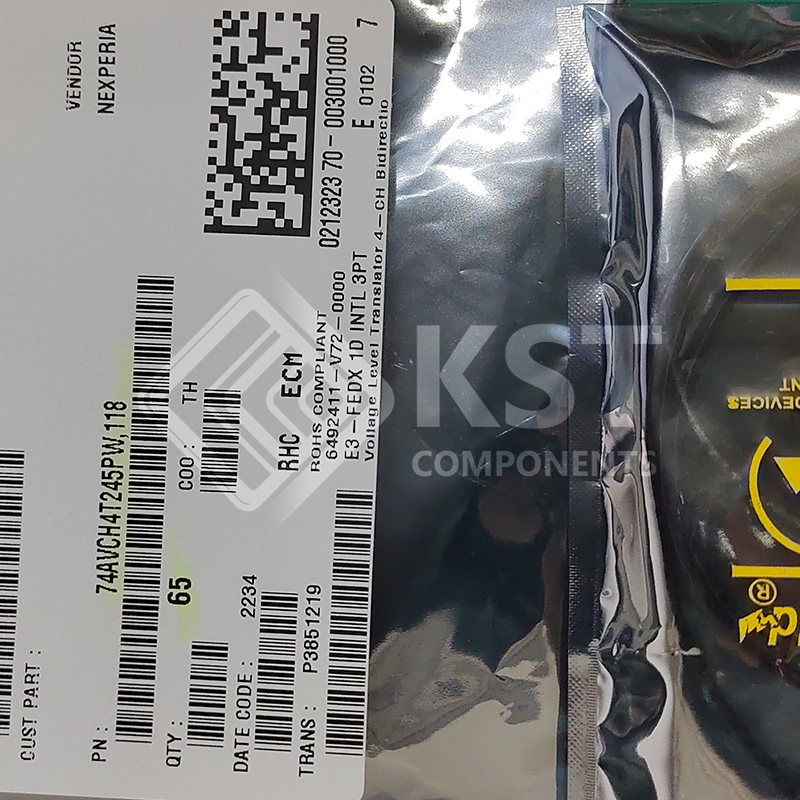
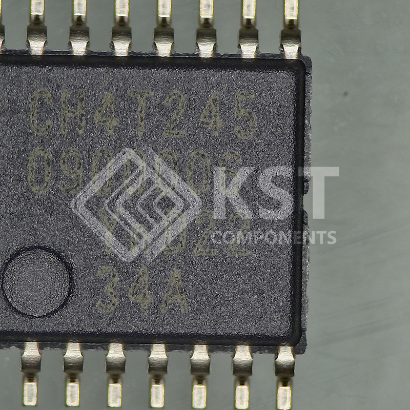
74AVCH4T245PW,118

The 74AVCH4T245 is a 4-bit, dual supply transceiver that enables bidirectional level translation.
The device can be used as two 2-bit transceivers or as a 4-bit transceiver. It features two 2-bit
input-output ports (nAn and nBn), a direction control input (nDIR), an output enable input (nOE)
and dual supply pins (VCC(A) and VCC(B)). Both VCC(A) and VCC(B) can be supplied at any voltage
between 0.8 V and 3.6 V making the device suitable for translating between any of the low voltage
nodes (0.8 V, 1.2 V, 1.5 V, 1.8 V, 2.5 V and 3.3 V). Pins nAn, nOE and nDIR are referenced to
VCC(A) and pins nBn are referenced to VCC(B). A HIGH on nDIR allows transmission from nAn to
nBn and a LOW on nDIR allows transmission from nBn to nAn. The output enable input (nOE) can
be used to disable the outputs so the buses are effectively isolated.
The device is fully specified for partial power-down applications using IOFF. The IOFF circuitry
disables the output, preventing any damaging backflow current through the device when it is
powered down. In suspend mode when either VCC(A) or VCC(B) are at GND level, both nAn and
nBn outputs are in the high-impedance OFF-state. The bus hold circuitry on the powered-up side
always stays active.
The 74AVCH4T245 has active bus hold circuitry which is provided to hold unused or floating data
inputs at a valid logic level. This feature eliminates the need for external pull-up or pull-down
resistors.

Category:

Download Details PDF

Notice:

In stock will ship in 2 days. Real-time inventory pls confirm with us.

INQUIRY ONLINE


    SPECIFICATION

    • Wide supply voltage range: VCC(A): 0.8 V to 3.6 V; VCC(B): 0.8 V to 3.6 V
    • Complies with JEDEC standards:
    • JESD8-12 (0.8 V to 1.3 V)
    • JESD8-11 (0.9 V to 1.65 V)
    • JESD8-7 (1.2 V to 1.95 V)
    • JESD8-5 (1.8 V to 2.7 V)
    • JESD8-B (2.7 V to 3.6 V)
    • Maximum data rates:
    • 380 Mbit/s (≥ 1.8 V to 3.3 V translation)
    • 200 Mbit/s (≥ 1.1 V to 3.3 V translation)
    • 200 Mbit/s (≥ 1.1 V to 2.5 V translation)
    • 200 Mbit/s (≥ 1.1 V to 1.8 V translation)
    • 150 Mbit/s (≥ 1.1 V to 1.5 V translation)
    • 100 Mbit/s (≥ 1.1 V to 1.2 V translation)
    • Suspend mode
    • Bus hold on data inputs
    • Latch-up performance exceeds 100 mA per JESD 78 Class II
    • Inputs accept voltages up to 3.6 V
    • IOFF circuitry provides partial Power-down mode operation
    • ESD protection:
    • HBM: ANSI/ESDA/JEDEC JS-001 class 3B exceeds 8000 V
    • CDM: ANSI/ESDA/JEDEC JS-002 class C3 exceeds 1000 V
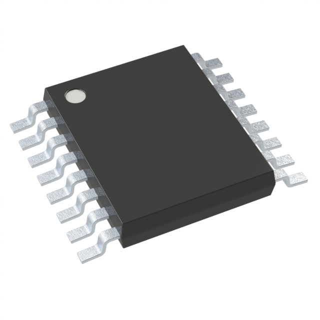
    • Multiple package options
    • Specified from -40 °C to +85 °C and -40 °C to +125 °C