


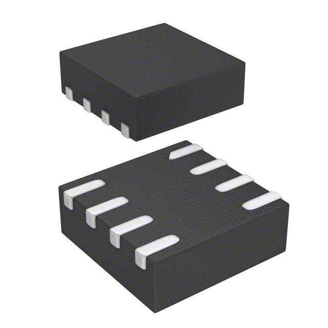
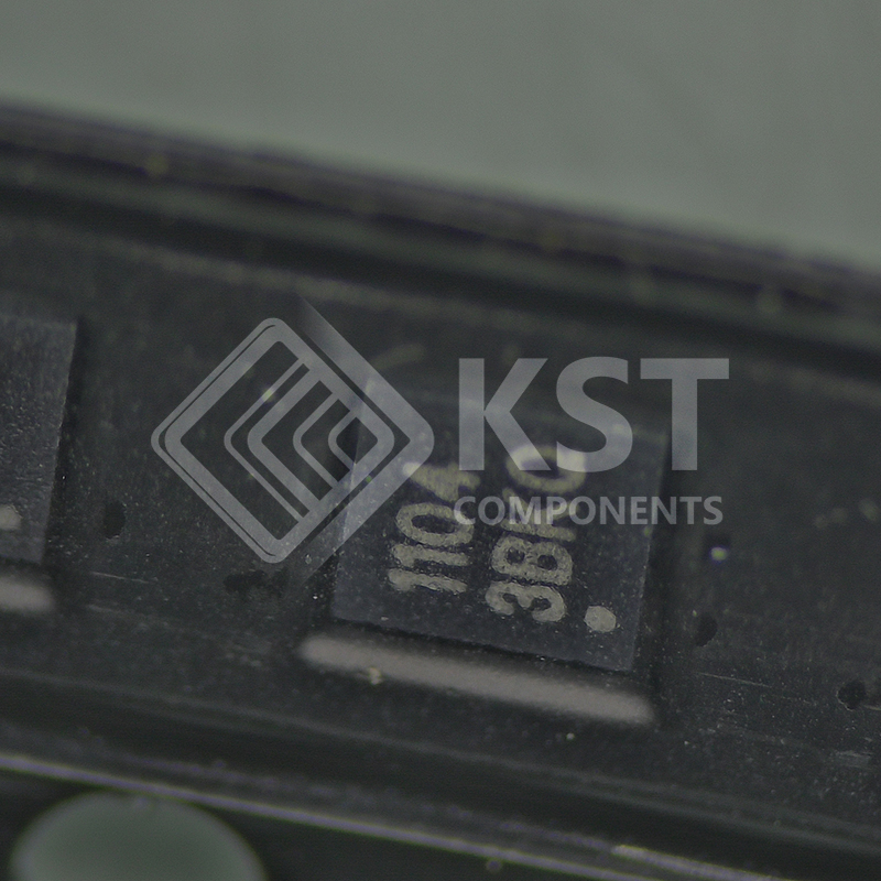
5PB1104CMGI
INQUIRY ONLINE
High-performance 1:2, 1:4, 1:6, 1:8, 1:10 LVCMOS clock buffer
▪ Very low pin-to-pin skew: < 50ps
▪ Very low additive jitter: < 50fs
▪ Supply voltage: 1.8V to 3.3V
▪ 3.3V tolerant input clock
▪ f
MAX = 200MHz
▪ Integrated serial termination for 50Ω channel
▪ Packaged in 8-, 14-, 16-, 20-pin TSSOP and as small as
2.0 × 2.0 mm DFN and 3.0 × 3.0 mm VFQFPN packages
▪ Industrial (-40°C to +85°C) and extended (-40°C to +105°C)
temperature ranges
▪ 5PB1104 available in AEC-Q100 qualified, Automotive Grade 1
(-40°C to +125°C)
▪ 5PB1110 available in AEC-Q100 qualified, Automotive Grade 2
(-40°C to +105°C)