


1P1G125QDCKRQ1
INQUIRY ONLINE
• AEC-Q100 Qualified With the Following Results:
– Device Temperature Grade 1: –40°C to +125°C
Ambient Operating Temperature Range
– Device Human-Body Model (HBM) ESD
Classification Level 2
– Device Charged-Device Model (CDM) ESD
Classification Level C5
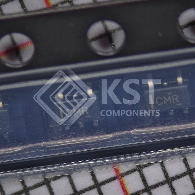
• Available in the small 1.45-mm2
package (DRY) With 0.5-mm Pitch
• Supports 5-V VCC Operation
• Over-voltage tolerant inputs accept
voltages to 5.5 V
• Provides down translation to VCC
• Max tpd of 3.7 ns at 3.3 V
• Low power consumption, 10-μA Max ICC
• ±24-mA Output drive at 3.3 V
• Ioff supports live insertion, partial-power-down
mode, and back-drive protection
• Latch-up performance exceeds 100 mA
Per JESD 78, Class II