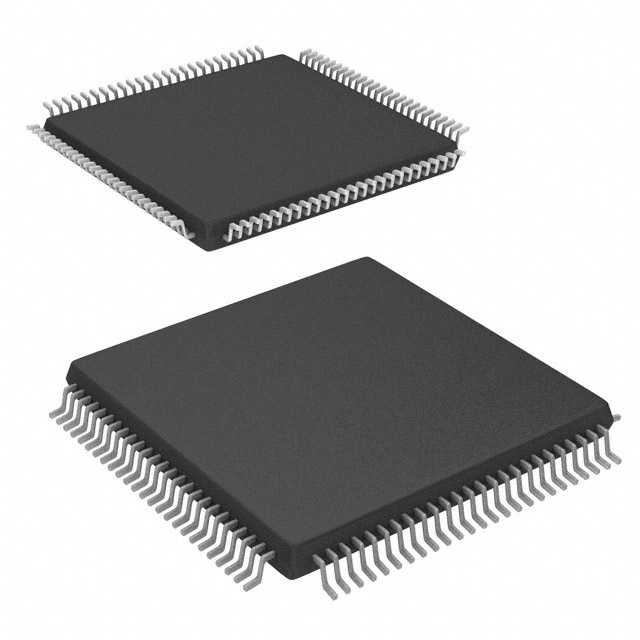
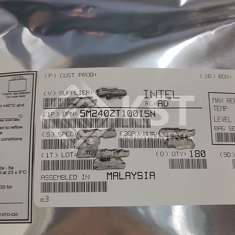
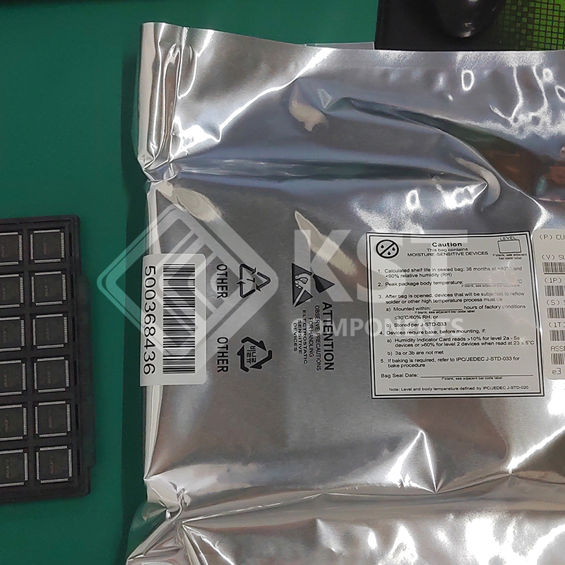
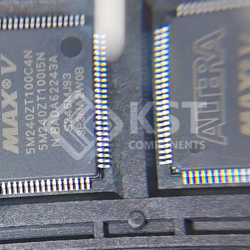
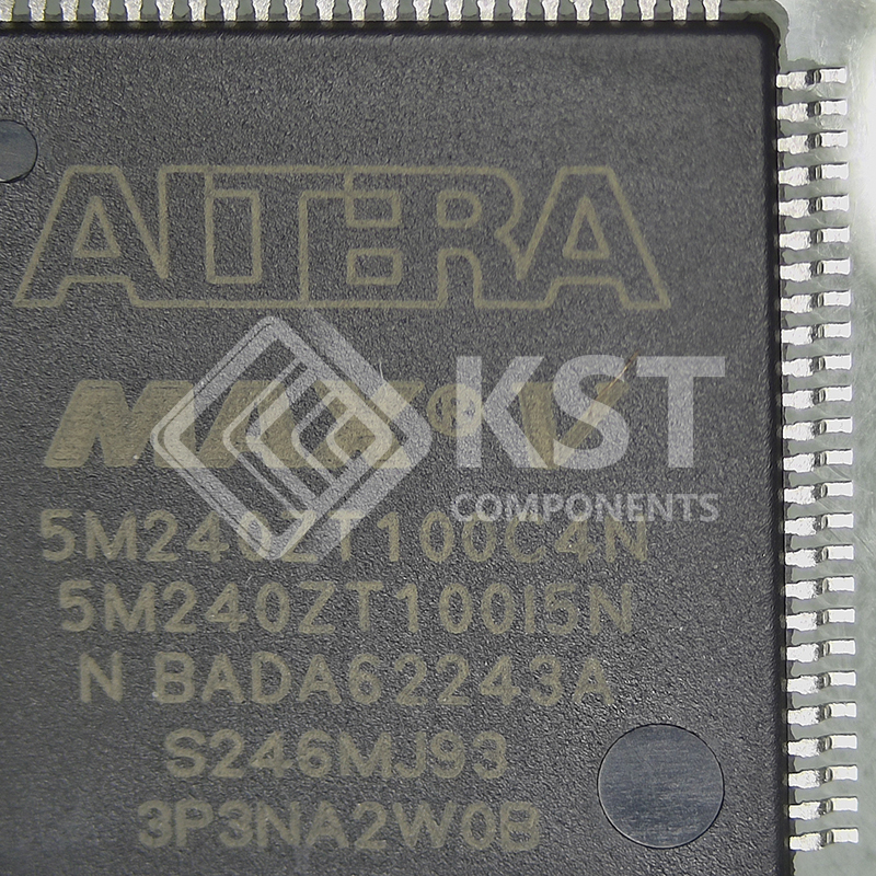
5M240ZT100I5N

MAX V devices contain a two-dimensional row- and column-based architecture to
implement custom logic. Row and column interconnects provide signal interconnects
between the logic array blocks (LABs).
Each LAB in the logic array contains 10 logic elements (LEs). An LE is a small unit of
logic that provides efficient implementation of user logic functions. LABs are grouped
into rows and columns across the device. The MultiTrack interconnect provides fast
granular timing delays between LABs. The fast routing between LEs provides
minimum timing delay for added levels of logic versus globally routed interconnect
structures.
The I/O elements (IOEs) located after the LAB rows and columns around the
periphery of the MAX V device feeds the I/O pins. Each IOE contains a bidirectional
I/O buffer with several advanced features. I/O pins support Schmitt trigger inputs
and various single-ended standards, such as 33-MHz, 32-bit PCI™, and LVTTL.
MAX V devices provide a global clock network. The global clock network consists of
four global clock lines that drive throughout the entire device, providing clocks for all
resources within the device. You can also use the global clock lines for control signals
such as clear, preset, or output enable.


Download Details PDF

Notice:

In stock will ship in 2 days. Real-time inventory pls confirm with us.

INQUIRY ONLINE


    SPECIFICATION

    The following list summarizes the MAX V device family features:
    ■ Low-cost, low-power, and non-volatile CPLD architecture
    ■ Instant-on (0.5 ms or less) configuration time
    ■ Standby current as low as 25 µA and fast power-down/reset operation
    ■ Fast propagation delay and clock-to-output times
    ■ Internal oscillator
    ■ Emulated RSDS output support with a data rate of up to 200 Mbps
    ■ Emulated LVDS output support with a data rate of up to 304 Mbps
    ■ Four global clocks with two clocks available per logic array block (LAB)
    ■ User flash memory block up to 8 Kbits for non-volatile storage with up to 1000
    read/write cycles
    ■ Single 1.8-V external supply for device core
    ■ MultiVolt I/O interface supporting 3.3-V, 2.5-V, 1.8-V, 1.5-V, and 1.2-V logic levels
    ■ Bus-friendly architecture including programmable slew rate, drive strength,
    bus-hold, and programmable pull-up resistors
    ■ Schmitt triggers enabling noise tolerant inputs (programmable per pin)

    ■ I/Os are fully compliant with the PCI-SIG® PCI Local Bus Specification, revision
    2.2 for 3.3-V operation
    ■ Hot-socket compliant
    ■ Built-in JTAG BST circuitry compliant with IEEE Std. 1149.1-1990