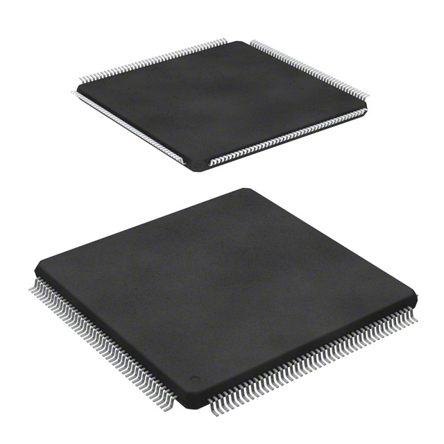
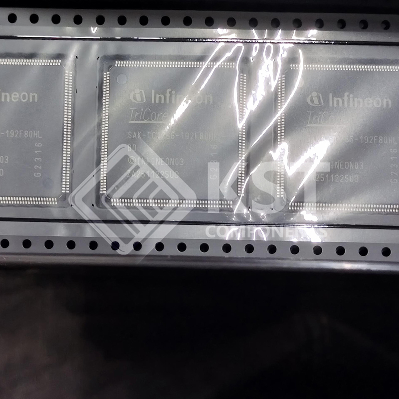
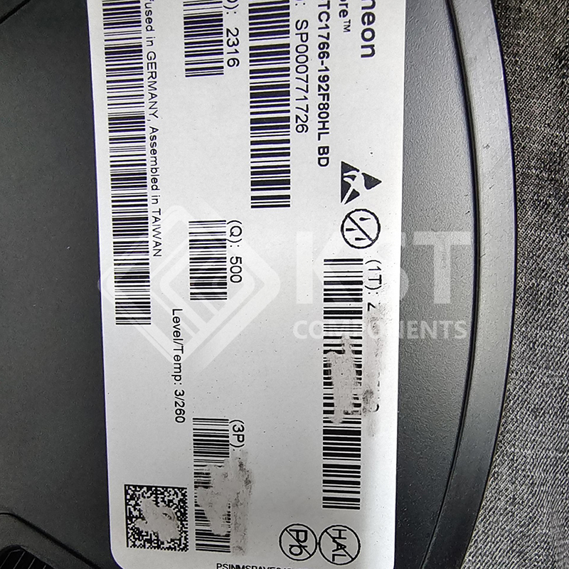
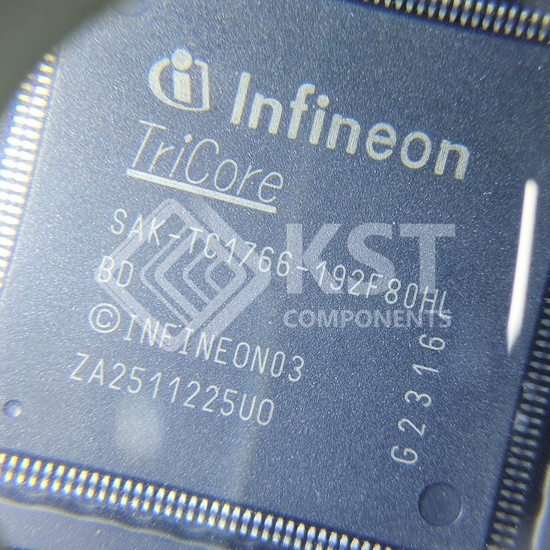
SAK-TC1766-192F80HLBD

The TC1766 has two independent on-chip buses (see also TC1766 block diagram on
Page 2-6):
• Local Memory Bus (LMB)
• System Peripheral Bus (SPB)
The LMB Bus connects the CPU local resources for data and instruction fetch. The Local
Memory Bus interconnects the memory units and functional units, such as CPU and
PMU. The main target of the LMB bus is to support devices with fast response times,
optimized for speed. This allows the DMI and PMI fast access to local memory and
reduces load on the FPI bus. The Tricore system itself is located on LMB bus.
The Local Memory Bus is a synchronous, pipelined, split bus with variable block size
transfer support. It supports 8-, 16-, 32- and 64-bit single transactions and variable
length 64-bit block transfers.
The SPB Bus is mainly governed by the PCP and is accessible to the CPU via the LMB
Bus bridge. The System Peripheral Bus (SPB Bus) in TC1766 is an on-chip FPI Bus. The
FPI Bus interconnects the functional units of the TC1766, such as the DMA and on-chip
peripheral components. The FPI Bus is designed to be quick to be acquired by on-chip
functional units, and quick to transfer data. The low setup overhead of the FPI Bus
access protocol guarantees fast FPI Bus acquisition, which is required for time-critical
applications.The FPI Bus is designed to sustain high transfer rates. For example, a peak
transfer rate of up to 320 Mbyte/s can be achieved with a 80 MHz bus clock and 32-bit
data bus. Multiple data transfers per bus arbitration cycle allow the FPI Bus to operate
at close to its peak bandwidth.
Both the LMB Bus and the SPB Bus runs at full CPU speed. The maximum CPU speed
is 80 MHz.
Additionally, two simplified bus interfaces are connected to and controlled by the DMA
Controller:
• DMA Bus
• SMIF Interface


Download Details PDF

Notice:

In stock will ship in 2 days. Real-time inventory pls confirm with us.

INQUIRY ONLINE


    SPECIFICATION

    The TC1766 has the following features:
    • High-performance 32-bit super-scaler TriCore v1.3 CPU with 4-stage pipeline
    – Superior real-time performance
    – Strong bit handling
    – Fully integrated DSP capabilities
    – Single precision Floating Point Unit (FPU)
    – 80 MHz operation at full temperature range
    • Peripheral Control Processor with single cycle instruction (PCP2)
    – 8 Kbyte Parameter Memory (PRAM)
    – 12 Kbyte Code Memory (CMEM)
    • Multiple on-chip memories
    – 56 Kbyte Local Data Memory (SRAM)
    – 8 Kbyte Overlay Memory
    – 16 Kbyte Scratch-Pad RAM (SPRAM)
    – 8 Kbyte Instruction Cache (ICACHE)
    – 1504 Kbyte Program Flash (for instruction code and constant data)
    – 32 Kbyte Data Flash (e.g. 4 Kbyte EEPROM emulation)
    – 16 Kbyte Boot ROM
    • 8-channel DMA Controller
    • Fast-response interrupt system with 2 x 255 hardware priority arbitration levels
    serviced by CPU or PCP2
    • High-performance on-chip bus structure
    – 64-bit Local Memory Bus (LMB) to Flash memory
    – System Peripheral Bus (SPB) for interconnections of functional units
    • Versatile on-chip Peripheral Units
    – Two Asynchronous/Synchronous Serial Channels (ASCs) with baudrate
    generator, parity, framing and overrun error detection
    – Two High Speed Synchronous Serial Channels (SSCs) with programmable data
    length and shift direction
    – One Micro Second Bus (MSC) interface for serial port expansion to external power
    devices
    – Two high-speed Micro Link Interfaces (MLIs) for serial inter-processor
    communication
    – One MultiCAN Module with two CAN nodes and 64 free assignable message
    objects for high efficiency data handling via FIFO buffering and gateway data
    transfer
    – One General Purpose Timer Array Module (GPTA) with a powerful set of digital
    signal filtering and timer functionality to realize autonomous and complex
    Input/Output management
    – One 16-channel Analog-to-Digital Converter unit (ADC) with selectable 8-bit, 10-
    bit, or 12-bit, supporting 32 input channels