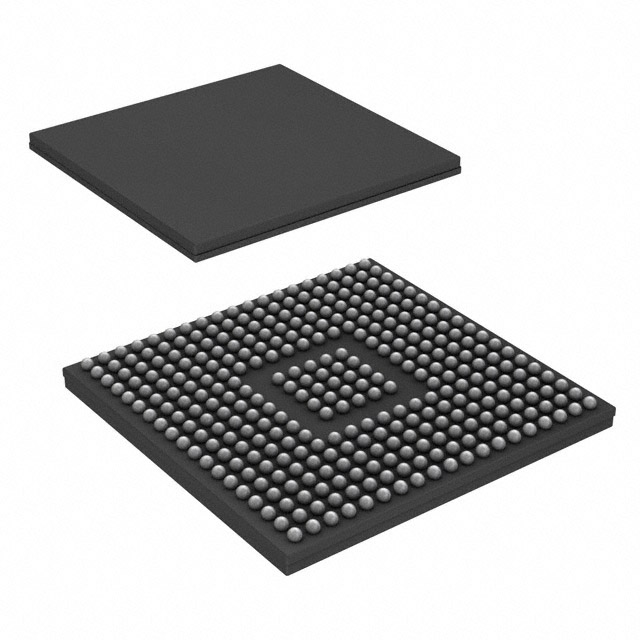
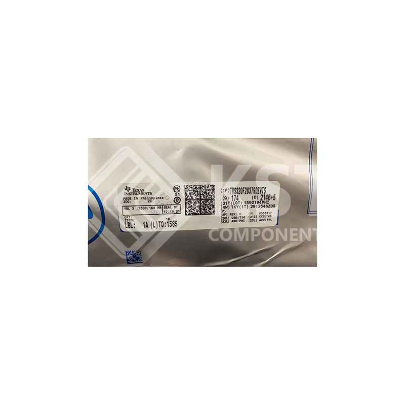
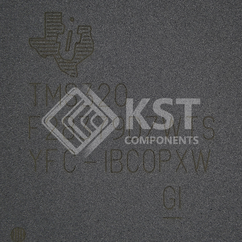
TMS320F28379DZWTS

C2000™ 32-bit microcontrollers are optimized for processing, sensing, and actuation to improve closed-loop
performance in real-time control applications such as industrial motor drives; solar inverters and digital power;
electrical vehicles and transportation; motor control; and sensing and signal processing. The C2000 line includes
the Premium performance MCUs and the Entry performance MCUs.
The TMS320F2837xD is a powerful 32-bit floating-point microcontroller unit (MCU) designed for advanced
closed-loop control applications such as industrial motor drives; solar inverters and digital power; electrical
vehicles and transportation; and sensing and signal processing. To accelerate application development, the
DigitalPower software development kit (SDK) for C2000 MCUs and the MotorControl software development
kit (SDK) for C2000™ MCUs are available. The F2837xD supports a new dual-core C28x architecture that
significantly boosts system performance. The integrated analog and control peripherals also let designers
consolidate control architectures and eliminate multiprocessor use in high-end systems.
The dual real-time control subsystems are based on TI’s 32-bit C28x floating-point CPUs, which provide
200MHz of signal processing performance in each core. The C28x CPUs are further boosted by the new TMU
accelerator, which enables fast execution of algorithms with trigonometric operations common in transforms and
torque loop calculations; and the VCU accelerator, which reduces the time for complex math operations common
in encoded applications.
The F2837xD microcontroller family features two CLA real-time control coprocessors. The CLA is an
independent 32-bit floating-point processor that runs at the same speed as the main CPU. The CLA responds to
peripheral triggers and executes code concurrently with the main C28x CPU. This parallel processing capability
can effectively double the computational performance of a real-time control system. By using the CLA to
service time-critical functions, the main C28x CPU is free to perform other tasks, such as communications and
diagnostics. The dual C28x+CLA architecture enables intelligent partitioning between various system tasks. For
example, one C28x+CLA core can be used to track speed and position, while the other C28x+CLA core can be
used to control torque and current loops.

The TMS320F2837xD supports up to 1MB (512KW) of onboard flash memory with error correction code (ECC)
and up to 204KB (102KW) of SRAM. Two 128-bit secure zones are also available on each CPU for code
protection.
Performance analog and control peripherals are also integrated on the F2837xD MCU to further enable
system consolidation. Four independent 16-bit ADCs provide precise and efficient management of multiple
analog signals, which ultimately boosts system throughput. The new sigma-delta filter module (SDFM) works
in conjunction with the sigma-delta modulator to enable isolated current shunt measurements. The Comparator
Subsystem (CMPSS) with windowed comparators allows for protection of power stages when current limit
conditions are exceeded or not met. Other analog and control peripherals include DACs, PWMs, eCAPs,
eQEPs, and other peripherals.
Peripherals such as EMIFs, CAN modules (ISO 11898-1/CAN 2.0B-compliant), and a new uPP interface extend
the connectivity of the F2837xD. The uPP interface is a new feature of the C2000™ MCUs and supports
high-speed parallel connection to FPGAs or other processors with similar uPP interfaces. Lastly, a USB 2.0 port
with MAC and PHY lets users easily add universal serial bus (USB) connectivity to their application.
Want to learn more about features that make C2000 MCUs the right choice for your real-time control system?
Check out The Essential Guide for Developing With C2000™ Real-Time Microcontrollers and visit the C2000™
real-time control MCUs page.
The Getting Started With C2000™ Real-Time Control Microcontrollers (MCUs) Getting Started Guide covers all
aspects of development with C2000 devices from hardware to support resources. In addition to key reference
documents, each section provides relevant links and resources to further expand on the information covered.
Ready to get started? Check out the TMDSCNCD28379D or LAUNCHXL-F28379D evaluation board sand
download C2000Ware.
To learn more about the C2000 MCUs, visit the C2000 Overview at www.ti.com/c2000.


Download Details PDF

Notice:

In stock will ship in 2 days. Real-time inventory pls confirm with us.

INQUIRY ONLINE


    SPECIFICATION

    • Dual-core architecture
    – Two TMS320C28x 32-bit CPUs
    – 200MHz
    – IEEE 754 single-precision Floating-Point Unit
    (FPU)
    – Trigonometric Math Unit (TMU)
    – Viterbi/Complex Math Unit (VCU-II)
    • Two programmable Control Law Accelerators
    (CLAs)
    – 200MHz
    – IEEE 754 single-precision floating-point
    instructions
    – Executes code independently of main CPU
    • On-chip memory
    – 512KB (256KW) or 1MB (512KW) of flash
    (ECC-protected)
    – 172KB (86KW) or 204KB (102KW) of RAM
    (ECC-protected or parity-protected)
    – Dual-zone security supporting third-party
    development
    – Unique identification number
    • Clock and system control
    – Two internal zero-pin 10MHz oscillators
    – On-chip crystal oscillator
    – Windowed watchdog timer module
    – Missing clock detection circuitry
    • 1.2V core, 3.3V I/O design
    • System peripherals
    – Two External Memory Interfaces (EMIFs) with
    ASRAM and SDRAM support
    – Dual 6-channel Direct Memory Access (DMA)
    controllers
    – Up to 169 individually programmable,
    multiplexed General-Purpose Input/Output
    (GPIO) pins with input filtering
    – Expanded Peripheral Interrupt controller (ePIE)
    – Multiple Low-Power Mode (LPM) support with
    external wakeup
    • Communications peripherals
    – USB 2.0 (MAC + PHY)
    – Support for 12-pin 3.3V-compatible Universal
    Parallel Port (uPP) interface
    – Two Controller Area Network (CAN) modules
    (pin-bootable)
    – Three high-speed (up to 50MHz) SPI ports (pinbootable)
    – Two Multichannel Buffered Serial Ports
    (McBSPs)
    – Four Serial Communications Interfaces (SCI/
    UART) (pin-bootable)
    – Two I2C interfaces (pin-bootable)
    • Analog subsystem
    – Up to four Analog-to-Digital Converters (ADCs)
    • 16-bit mode
    – 1.1MSPS each (up to 4.4MSPS system
    throughput)
    – Differential inputs
    – Up to 12 external channels
    • 12-bit mode
    – 3.5MSPS each (up to 14MSPS system
    throughput)
    – Single-ended inputs
    – Up to 24 external channels
    • Single Sample-and-Hold (S/H) on each ADC
    • Hardware-integrated post-processing of
    ADC conversions
    – Saturating offset calibration
    – Error from setpoint calculation
    – High, low, and zero-crossing compare,
    with interrupt capability
    – Trigger-to-sample delay capture
    – Eight windowed comparators with 12-bit Digitalto-Analog Converter (DAC) references
    – Three 12-bit buffered DAC outputs
    • Enhanced control peripherals
    – 24 Pulse Width Modulator (PWM) channels with
    enhanced features
    – 16 High-Resolution Pulse Width Modulator
    (HRPWM) channels
    • High resolution on both A and B channels of
    8 PWM modules
    • Dead-band support (on both standard and
    high resolution)
    – Six Enhanced Capture (eCAP) modules
    – Three Enhanced Quadrature Encoder Pulse
    (eQEP) modules
    – Eight Sigma-Delta Filter Module (SDFM) input
    channels, 2 parallel filters per channel
    • Standard SDFM data filtering
    • Comparator filter for fast action for out of
    range
    • Configurable Logic Block (CLB)
    – Augments existing peripheral capability
    – Supports position manager solutions

    • Functional Safety-Compliant
    – Developed for functional safety applications
    – Documentation available to aid ISO 26262
    system design up to ASIL D; IEC 61508 up to
    SIL 3; IEC 60730 up to Class C; and UL 1998
    up to Class 2
    – Hardware integrity up to ASIL B, SIL 2
    • Safety-related certification
    – ISO 26262 certified up to ASIL B and IEC
    61508 certified up to SIL 2 by TUV SUD
    • Package options:
    – Lead-free, green packaging
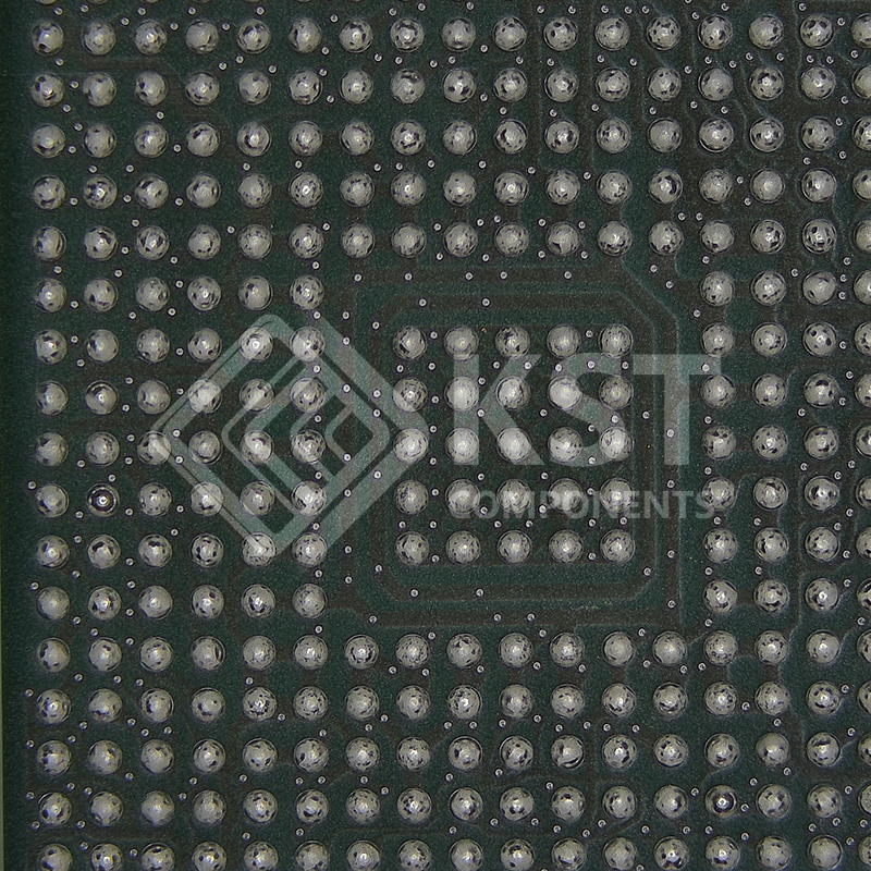
    – 337-ball New Fine Pitch Ball Grid Array
    (nFBGA) [ZWT suffix]
    – 176-pin PowerPAD™ Thermally Enhanced LowProfile Quad Flatpack (HLQFP) [PTP suffix]
    – 100-pin PowerPAD Thermally Enhanced Thin
    Quad Flatpack (HTQFP) [PZP suffix]
    • Hardware Built-in Self Test (HWBIST)
    • Temperature options:
    – T: –40°C to 105°C junction
    – S: –40°C to 125°C junction
    – Q: –40°C to 125°C free-air
    (AEC Q100 qualification for automotive
    applications)