CYD36S36V18-167BGXI

The FullFlex™ dual port SRAM families consist of 2-Mbit, 9-Mbit,
18-Mbit, and 36-Mbit synchronous, true dual-port static RAMs
that are high-speed, low-power 1.8 V or 1.5 V CMOS. Two ports
are provided, enabling simultaneous access to the array.
Simultaneous access to a location triggers deterministic access
control. For FullFlex72 these ports operate independently with
72-bit bus widths and each port is independently configured for
two pipelined stages. Each port is also configured to operate in
pipelined or flow through mode.
The advanced features include the following:
■ Built-in deterministic access control to manage address
collisions during simultaneous access to the same memory
location
■ Variable impedance matching (VIM) to improve data
transmission by matching the output driver impedance to the
line impedance
■ Echo clocks to improve data transfer
To reduce the static power consumption, chip enables power
down the internal circuitry. The number of latency cycles, before
a change in CE0 or CE1 enables or disables the databus,
matches the number of cycles of read latency selected for the
device. For a valid write or read to occur, activate both chip
enable inputs on a port.
Each port contains an optional burst counter on the input address
register. After externally loading the counter with the initial
address, the counter increments the address internally.
Additional device features include a mask register and a mirror
register to control counter increments and wrap around. The
counter interrupt (CNTINT) flags notify the host that the counter
reaches maximum count value on the next clock cycle. The host
reads the burst counter internal address, mask register address,
and busy address on the address lines. The host also loads the
counter with the address stored in the mirror register by using the
retransmit functionality. Mailbox interrupt flags are used for
message passing, and JTAG boundary scan and asynchronous
Master Reset (MRST) are also available. The Logic Block
Diagram on page 2 shows these features.
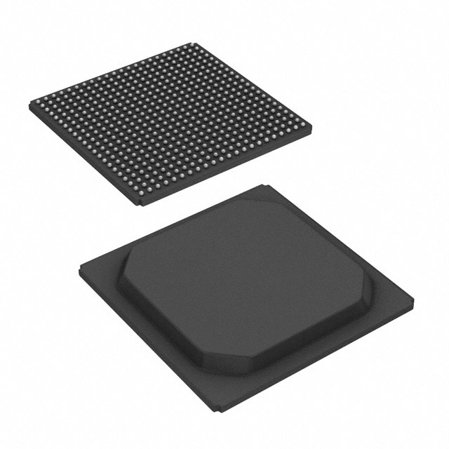
The FullFlex72 is offered in a 484-ball plastic BGA package. The
FullFlex36 and FullFlex18 are available in 256-ball fine pitch
BGA package except the 36-Mbit devices which are offered in
484-ball plastic BGA package.

Category:

Download Details PDF

Notice:

In stock will ship in 2 days. Real-time inventory pls confirm with us.

INQUIRY ONLINE


    SPECIFICATION

    ■ True dual port memory enables simultaneous access the
    shared array from each port
    ■ Synchronous pipelined operation with single data rate (SDR)
    operation on each port
    ❐ SDR interface at 200 MHz
    ❐ Up to 28.8 Gbps bandwidth (200 MHz × 72-bit × 2 ports)
    ■ Selectable pipelined or flow-through mode
    ■ 1.5 V or 1.8 V core power supply
    ■ Commercial and Industrial temperature
    ■ IEEE 1149.1 JTAG boundary scan
    ■ Available in 484-ball PBGA (× 72) and 256-ball FBGA (× 36
    and × 18) packages
    ■ FullFlex72 family
    ❐ 36-Mbit: 512K × 72 (CYD36S72V18)
    ❐ 18-Mbit: 256K × 72 (CYD18S72V18)
    ❐ 9-Mbit: 128K × 72 (CYD09S72V18)
    ■ FullFlex36 family
    ❐ 36-Mbit: 1M × 36 (CYD36S36V18)
    ❐ 18-Mbit: 512K × 36 (CYD18S36V18)
    ❐ 9-Mbit: 256K × 36 (CYD09S36V18)
    ❐ 2-Mbit: 64K × 36 (CYD02S36V18)
    ■ FullFlex18 family
    ❐ 36-Mbit: 2M × 18 (CYD36S18V18)
    ❐ 18-Mbit: 1M × 18 (CYD18S18V18)
    ❐ 9-Mbit: 512K × 18 (CYD09S18V18)
    ■ Built-in deterministic access control to manage address
    collisions
    ❐ Deterministic flag output upon collision detection
    ❐ Collision detection on back-to-back clock cycles
    ❐ First busy address readback
    ■ Advanced features for improved high-speed data transfer and
    flexibility
    ❐ Variable impedance matching (VIM)
    ❐ Echo clocks
    ❐ Selectable LVTTL (3.3 V), Extended HSTL[1] (1.4 V to 1.9 V),
    1.8 V LVCMOS, or 2.5 V LVCMOS I/O on each port
    ❐ Burst counters for sequential memory access
    ❐ Mailbox with interrupt flags for message passing
    ❐ Dual chip enables for easy depth expansion