


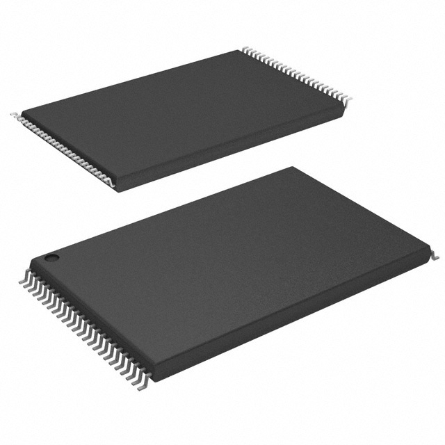
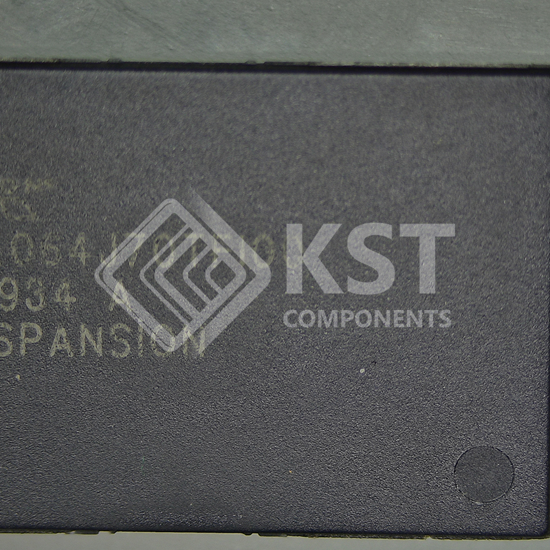
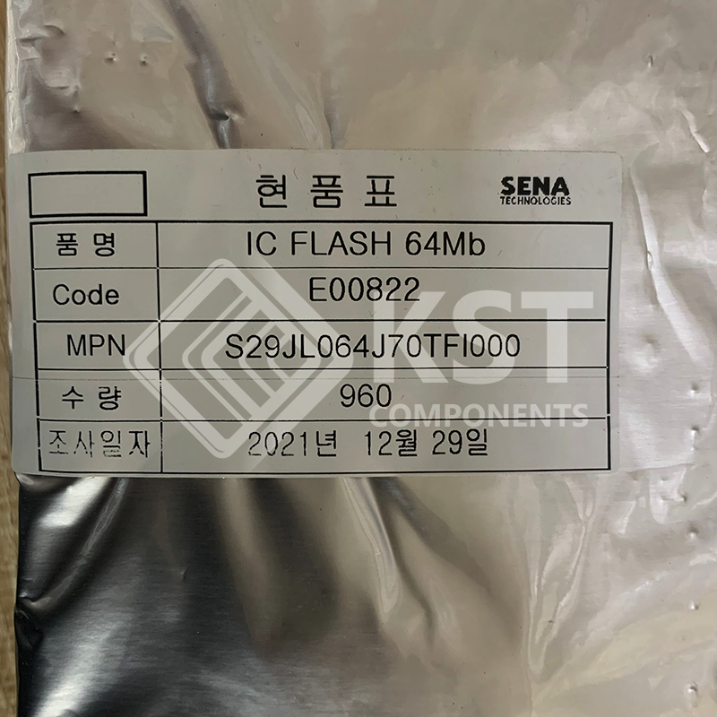
S29JL064J70TFI000
INQUIRY ONLINE
The Secured Silicon Region is an extra 256 byte sector capable of being permanently locked by Cypress or customers. The
Secured Silicon Customer Indicator Bit (DQ6) is permanently set to 1 if the part has been customer locked, and permanently set to 0
if the part has been factory locked. This way, customer lockable parts can never be used to replace a factory locked part.
Factory locked parts provide several options. The Secured Silicon Region may store a secure, random 16 byte ESN (Electronic
Serial Number), customer code (programmed through Cypress programming services), or both. Customer Lockable parts may
utilize the Secured Silicon Region as bonus space, reading and writing like any other flash sector, or may permanently lock their own
code there.
The device offers complete compatibility with the JEDEC 42.4 single-power-supply Flash command set standard. Commands
are written to the command register using standard microprocessor write timings. Reading data out of the device is similar to reading
from other Flash or EPROM devices.
The host system can detect whether a program or erase operation is complete by using the device status bits: RY/BY# pin, DQ7
(Data# Polling) and DQ6/DQ2 (toggle bits). After a program or erase cycle has been completed, the device automatically returns to
the read mode.
The sector erase architecture allows memory sectors to be erased and reprogrammed without affecting the data contents of other
sectors. The device is fully erased when shipped from the factory.
Hardware data protection measures include a low VCC detector that automatically inhibits write operations during power
transitions. The hardware sector protection feature disables both program and erase operations in any combination of the sectors
of memory. This can be achieved in-system or via programming equipment.
The Erase Suspend/Erase Resume feature enables the user to put erase on hold for any period of time to read data from, or
program data to, any sector that is not selected for erasure. True background erase can thus be achieved. If a read is needed from
the Secured Silicon Region (One Time Promgram area) after an erase suspend, then the user must use the proper command
sequence to enter and exit this region.
The device offers two power-saving features. When addresses have been stable for a specified amount of time, the device enters
the automatic sleep mode. The system can also place the device into the standby mode. Power consumption is greatly reduced in
both modes.