


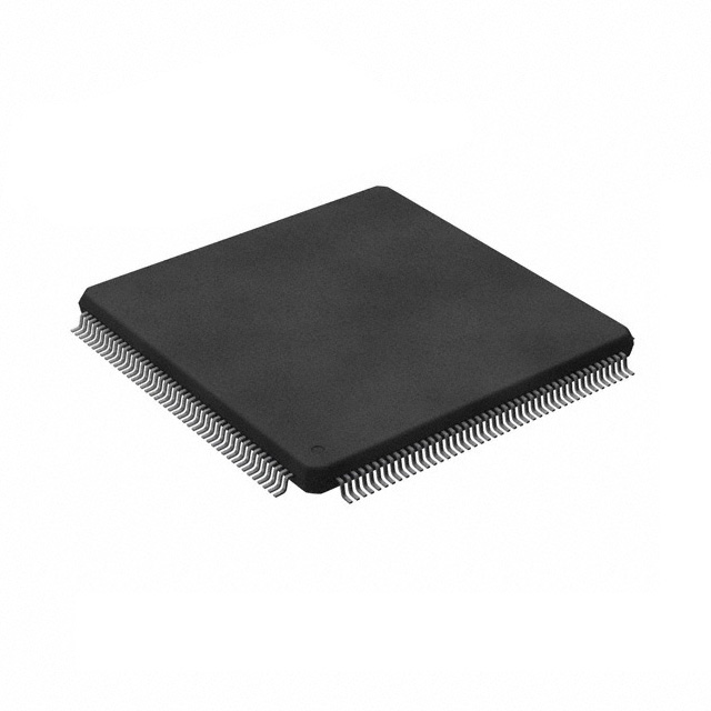


TMS320F2812PGFA
INQUIRY ONLINE
- High-performance static CMOS technology
- 150 MHz (6.67-ns cycle time)
- Low-power (1.8-V core at 135 MHz, 1.9-V core at 150 MHz, 3.3-V I/O) design
- JTAG boundary scan support
- IEEE Standard 1149.1-1990 IEEE Standard Test Access Port and Boundary-Scan Architecture
- High-performance 32-bit CPU (TMS320C28x)
- 16 × 16 and 32 × 32 MAC operations
- 16 × 16 dual MAC
- Harvard bus architecture
- Atomic operations
- Fast interrupt response and processing
- Unified memory programming model
- 4M linear program/data address reach
- Code-efficient (in C/C++ and Assembly)
- TMS320F24x/LF240x processor source code compatible
- On-chip memory
- Up to 128K × 16 flash (Four 8K × 16 and six 16K × 16 sectors)
- 1K × 16 OTP ROM
- L0 and L1: 2 blocks of 4K × 16 each Single-Access RAM (SARAM)
- H0: 1 block of 8K × 16 SARAM
- M0 and M1: 2 blocks of 1K × 16 each SARAM
- Boot ROM (4K × 16)
- With software boot modes
- Standard math tables
- External interface (F2812)
- Over 1M × 16 total memory
- Programmable wait states
- Programmable read/write strobe timing
- Three individual chip selects
- Endianness: Little endian
- Clock and system control
- On-chip oscillator
- Watchdog timer module
- Three external interrupts
- Peripheral Interrupt Expansion (PIE) block that supports 45 peripheral interrupts
- Three 32-bit CPU timers
- 128-bit security key/lock
- Protects flash/OTP and L0/L1 SARAM
- Prevents firmware reverse-engineering
- Motor control peripherals
- Two Event Managers (EVA, EVB)
- Compatible to 240xA devices
- Serial port peripherals
- Serial Peripheral Interface (SPI)
- Two Serial Communications Interfaces (SCIs), standard UART
- Enhanced Controller Area Network (eCAN)
- Multichannel Buffered Serial Port (McBSP)
- 12-bit ADC, 16 channels
- 2 × 8 channel input multiplexer
- Two Sample-and-Hold
- Single/simultaneous conversions
- Fast conversion rate: 80 ns/12.5 MSPS
- Up to 56 General-Purpose I/O (GPIO) pins
- Advanced emulation features
- Analysis and breakpoint functions
- Real-time debug via hardware
- Development tools include
- ANSI C/C++ compiler/assembler/linker
- Code Composer Studio™ IDE
- DSP/BIOS™
- JTAG scan controllers
- IEEE Standard 1149.1-1990 IEEE Standard Test Access Port and Boundary-Scan Architecture
- Low-power modes and power savings
- IDLE, STANDBY, HALT modes supported
- Disable individual peripheral clocks
- Package options
- 179-ball MicroStar BGA™ with external memory interface (GHH, ZHH) (F2812)
- 176-pin Low-Profile Quad Flatpack (LQFP) with external memory interface (PGF) (F2812)
- 128-pin LQFP without external memory interface (PBK) (F2810, F2811)
- Temperature options
- A: –40°C to 85°C (GHH, ZHH, PGF, PBK)
- S: –40°C to 125°C (GHH, ZHH, PGF, PBK)
- Q: –40°C to 125°C (PGF, PBK) (AEC-Q100 qualification for automotive applications)