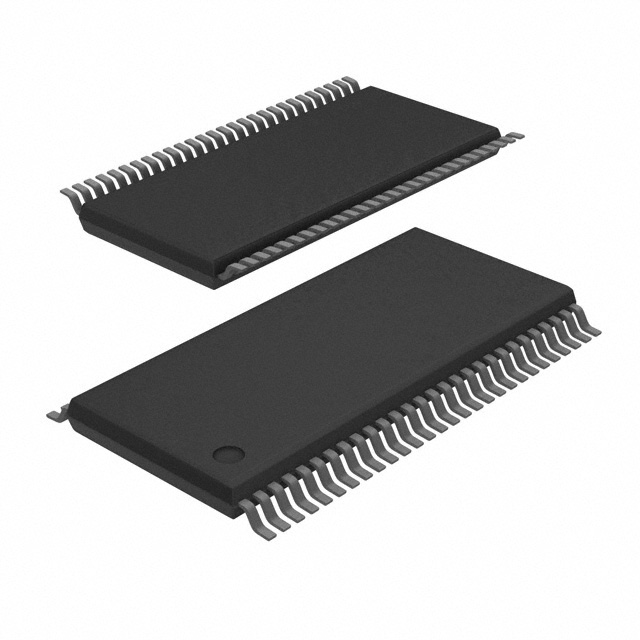
The SN75LVDS83B FlatLink™ transmitter contains four 7-bit parallel-load serial-out shift registers, a 7X clock synthesizer, and five Low-Voltage Differential Signaling (LVDS) line drivers in a single integrated circuit. These functions allow 28 bits of single-ended LVTTL data to be synchronously transmitted over five balanced-pair conductors for receipt by a compatible receiver, such as the SN75LVDS82 and LCD panels with integrated LVDS receiver.
When transmitting, data bits D0 through D27 are each loaded into registers upon the edge of the input clock signal (CLKIN). The rising or falling edge of the clock can be selected via the clock select (CLKSEL) pin. The frequency of CLKIN is multiplied seven times, and then used to unload the data registers in 7-bit slices and serially. The four serial streams and a phase-locked clock (CLKOUT) are then output to LVDS output drivers. The frequency of CLKOUT is the same as the input clock, CLKIN.
The SN75LVDS83B requires no external components and little or no control. The data bus appears the same at the input to the transmitter and output of the receiver with the data transmission transparent to the user(s). The only user intervention is selecting a clock rising edge by inputting a high level to CLKSEL or a falling edge with a low-level input, and the possible use of the Shutdown/Clear (SHTDN). SHTDN is an active-low input to inhibit the clock, and shut off the LVDS output drivers for lower power consumption. A low-level on this signal clears all internal registers to a low-level.
The SN75LVDS83B is characterized for operation over ambient air temperatures of –10°C to 70°C.
Alternative device option: The SN75LVDS83A (SLLS980) is an alternative to the SN75LVDS83B for clock frequency range of 10MHz-100MHz only. The SN75LVDS83A is available in the TSSOP package option only.
Download Details PDF
Notice:
In stock will ship in 2 days. Real-time inventory pls confirm with us.