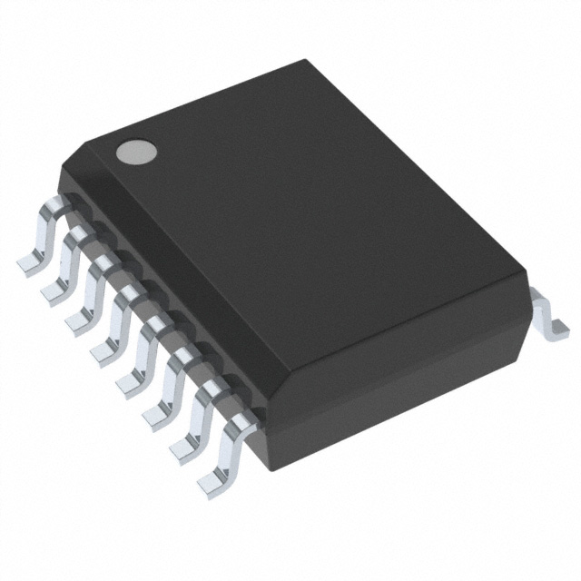
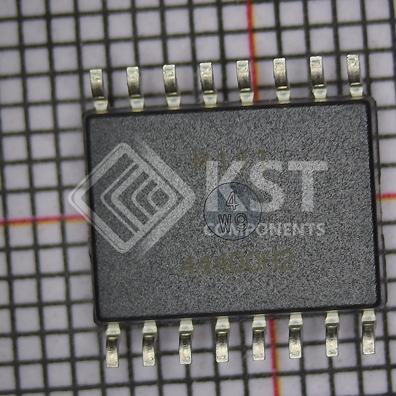
W25Q512JVFIQ

The W25Q512JV (512M-bit) Serial Flash memory provides a storage solution for systems with limited
space, pins and power. The 25Q series offers flexibility and performance well beyond ordinary Serial Flash
devices. They are ideal for code shadowing to RAM, executing code directly from Dual/Quad SPI (XIP)
and storing voice, text and data. The device operates on a single 2.7V to 3.6V power supply with current
consumption as low as 1µA for power-down. All devices are offered in space-saving packages.
The W25Q512JV array is organized into 262,144 programmable pages of 256-bytes each. Up to 256
bytes can be programmed at a time. Pages can be erased in groups of 16 (4KB sector erase), groups of
128 (32KB block erase), groups of 256 (64KB block erase) or the entire chip (chip erase). The
W25Q512JV has 16,384 erasable 4KB sectors and 1,028 erasable 64KB blocks respectively. The small
4KB sectors allow for greater flexibility in applications that require data and parameter storage.
The W25Q512JV supports the standard Serial Peripheral Interface (SPI), Dual/Quad I/O SPI: Serial Clock,
Chip Select, Serial Data I/O0 (DI), I/O1 (DO), I/O2, and I/O3. SPI clock frequencies of W25Q512JV of up
to 133MHz are supported allowing equivalent clock rates of 266MHz (133MHz x 2) for Dual I/O and
532MHz (133MHz x 4) for Quad I/O when using the Fast Read Dual/Quad I/O. These transfer rates can
outperform standard Asynchronous 8 and 16-bit Parallel Flash memories.
Additionally, the device supports JEDEC standard manufacturer and device ID and SFDP Register, a 64-
bit Unique Serial Number and three 256-bytes Security Registers.

Category:

Download Details PDF

Notice:

In stock will ship in 2 days. Real-time inventory pls confirm with us.

INQUIRY ONLINE


    SPECIFICATION

     New Family of SpiFlash Memories
    – W25Q512JV: 512M-bit / 64M-byte
    – Standard SPI: CLK, /CS, DI, DO
    – Dual SPI: CLK, /CS, IO0, IO1,
    – Quad SPI: CLK, /CS, IO0, IO1, IO2, IO3
    – 3 or 4-Byte Addressing Mode
    – Software & Hardware Reset(1)
     Highest Performance Serial Flash
    – 133MHz Standard/Dual/Quad SPI clocks
    – 266/532MHz equivalent Dual/Quad SPI
    – 66MB/S continuous data transfer rate
    – Min. 100K Program-Erase cycles per sector
    – More than 20-year data retention
     Efficient “Continuous Read”
    – Quad Peripheral Interface
    – Allows true XIP (execute in place) operation
    – Outperforms X16 Parallel Flash
     Low Power, Wide Temperature Range
    – Single 2.7 to 3.6V supply
    –<1µA Power-down (typ.)
    – -40°C to +85°C operating range
     Flexible Architecture with 4KB sectors
    – Uniform Sector/Block Erase (4K/32K/64K-Byte)
    – Program 1 to 256 byte per programmable page
    – Erase/Program Suspend & Resume
     Advanced Security Features
    – Software and Hardware Write-Protect
    – Power Supply Lock-Down
    – Special OTP protection
    – Top/Bottom, Complement array protection
    – Individual Block/Sector array protection
    – 64-Bit Unique ID for each device
    – Discoverable Parameters (SFDP) Register
    – 3X256-Bytes Security Registers with OTP locks
    – Volatile & Non-volatile Status Register Bits
     Space Efficient Packaging(2)
    – 8-pad WSON 8×6-mm
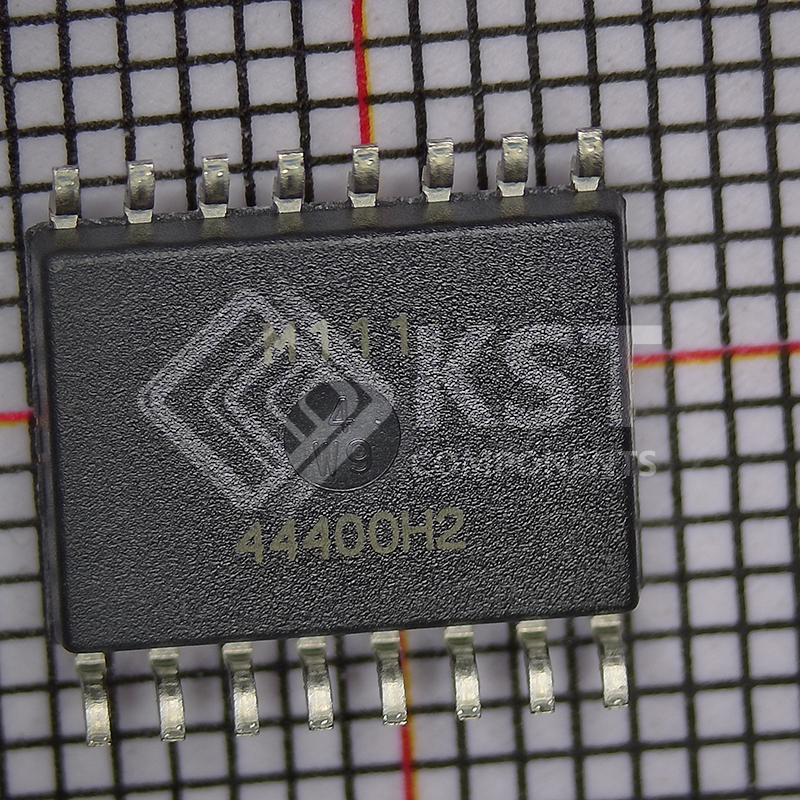
    – 16-pin SOIC 300-mil (additional /Reset pin)
    – 24-ball TFBGA 8×6-mm(5×5 ball array)
    – Contact Winbond for KGD and other options